

Thin film deposition apparatus, method of manufacturing organic light-emitting display device by using the thin film deposition apparatus, and organic light-emitting display device manufactured by using the method
a thin film deposition and manufacturing method technology, applied in the direction of spraying apparatus, coatings, vacuum evaporation coatings, etc., can solve the problems of distorting patterns, unsuitable deposition methods using such fmms, and not conducive to the recent trend towards high-definition patterns
- Summary
- Abstract
- Description
- Claims
- Application Information
AI Technical Summary
Benefits of technology
Problems solved by technology
Method used
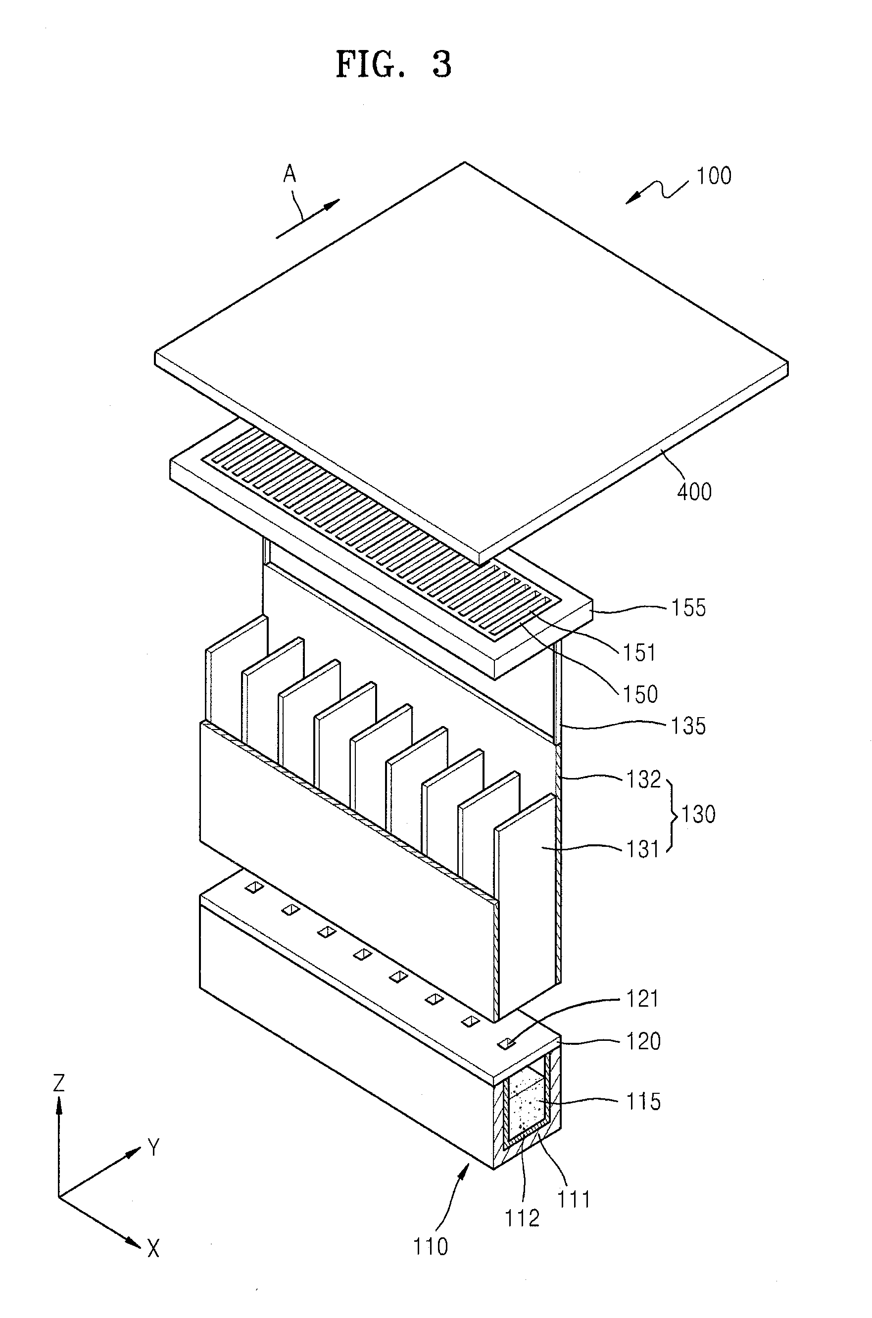
Image

Examples
Embodiment Construction
[0029]Hereinafter, the present invention will be described more fully with reference to the accompanying drawings, in which exemplary embodiments of the invention are shown. The invention may, however, be embodied in many different forms and should not be construed as being limited to the embodiments set forth herein; rather, these embodiments are provided so that this disclosure will be thorough and complete, and will fully convey the concept of the invention to those skilled in the art.
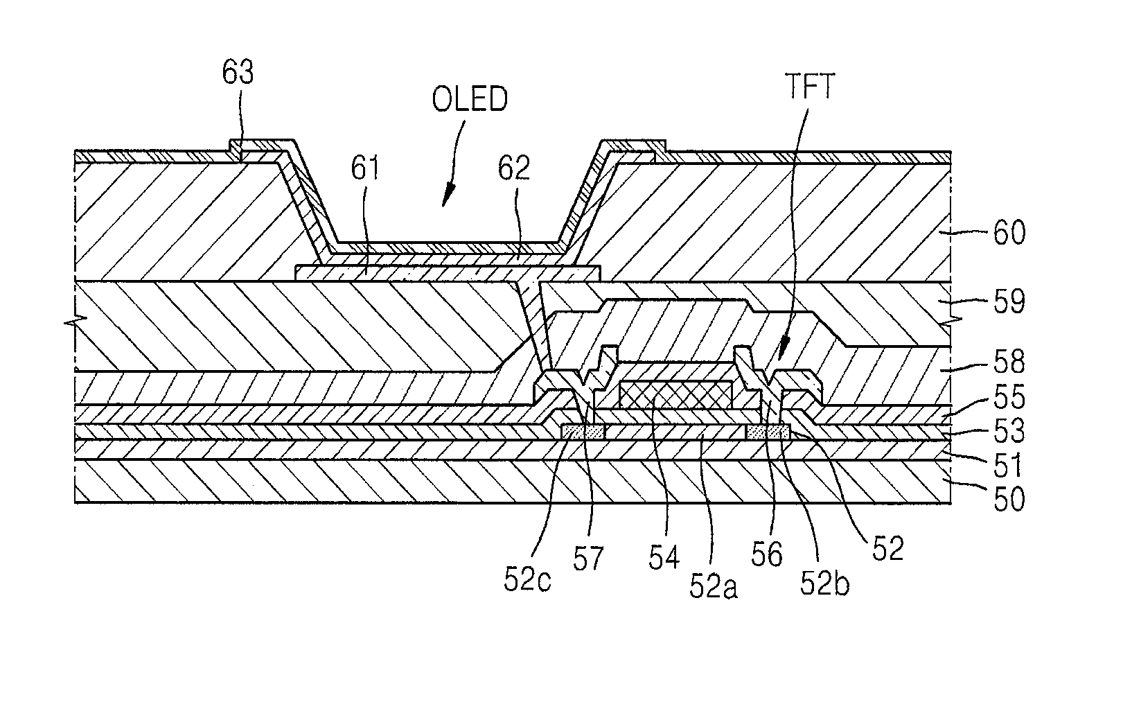
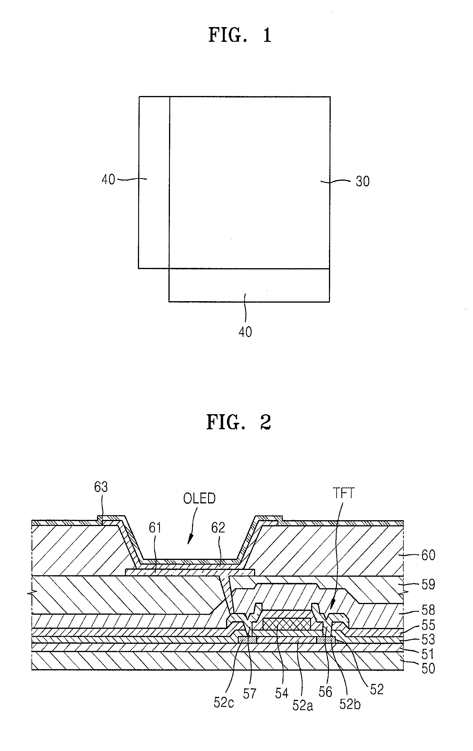
[0030]FIG. 1 is a plan view of an organic light-emitting display device manufactured by using a thin film deposition apparatus, according to an embodiment of the present invention.
[0031]Referring to FIG. 1, the organic light-emitting display device includes a pixel region (or display region) 30 and circuit regions 40 disposed at edges of the pixel region 30. The pixel region 30 includes a plurality of pixels, each of which includes an emission unit that emits light to display an image.
[0032]In an em...
PUM
| Property | Measurement | Unit |
|---|---|---|
| temperatures | aaaaa | aaaaa |
| temperature | aaaaa | aaaaa |
| temperature | aaaaa | aaaaa |
Abstract
Description
Claims
Application Information