Multilayer reflective film coated substrate, manufacturing method thereof, reflective mask blank, and reflective mask

Inactive Publication Date: 2007-04-26
HOYA CORP
View PDF3 Cites 26 Cited by
  • Summary
  • Abstract
  • Description
  • Claims
  • Application Information

AI Technical Summary

Benefits of technology

[0041] According to this invention, it is possible to provide a multilayer reflective film coated substrate having high surface smoothness and high reflectance which is suitable for a reflective mask for use in the lithography method using exposure light in a short wavelength region such as EUV light, and further provide a

Problems solved by technology

However, even if a glass polishing method of the current state is applied, it is actually quite difficult to obtain a highly smooth and defectless surface that can satisfy the foregoing surface r

Method used


Image

  • Multilayer reflective film coated substrate, manufacturing method thereof, reflective mask blank, and reflective mask
  • Multilayer reflective film coated substrate, manufacturing method thereof, reflective mask blank, and reflective mask
  • Multilayer reflective film coated substrate, manufacturing method thereof, reflective mask blank, and reflective mask

Examples


example 1

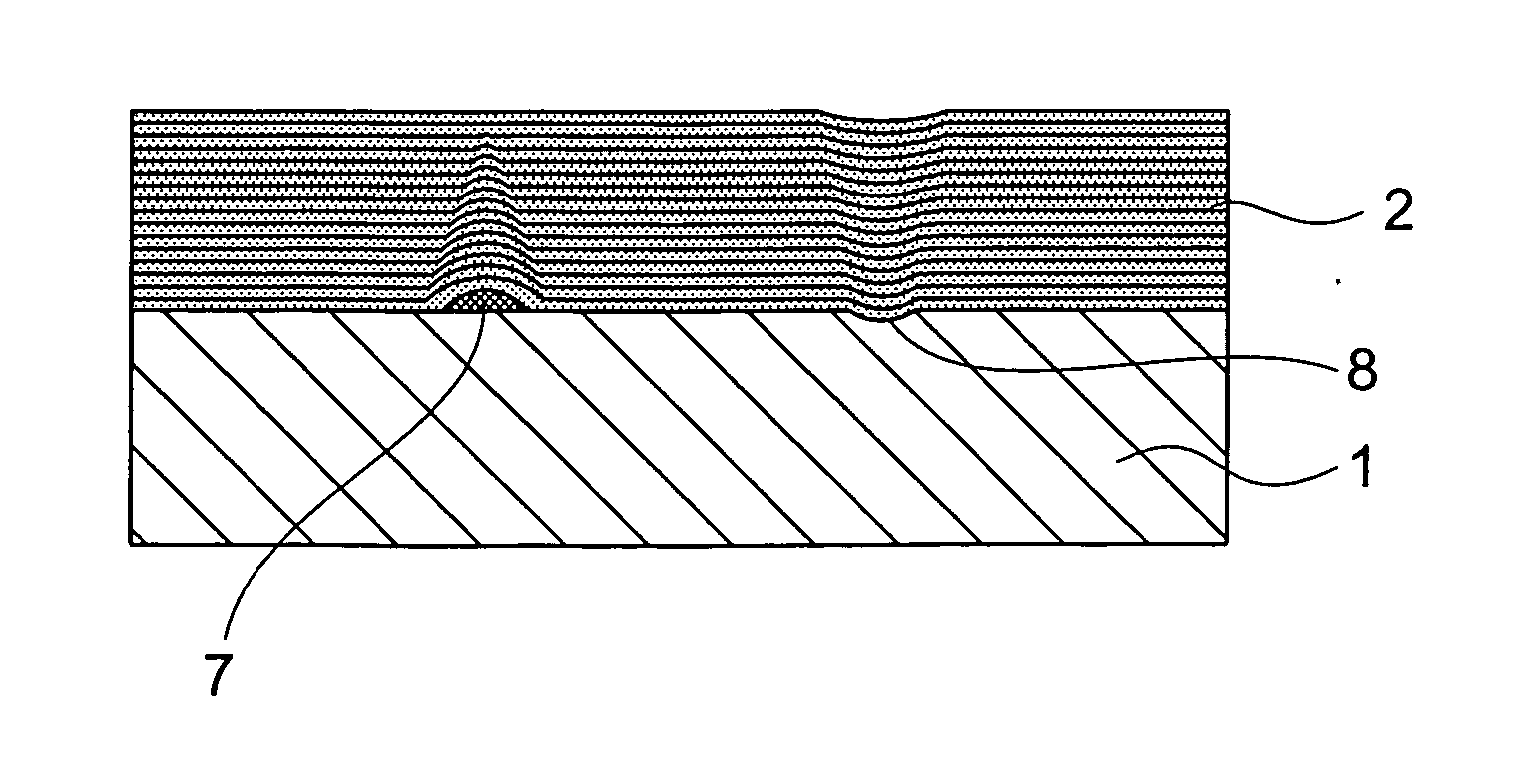
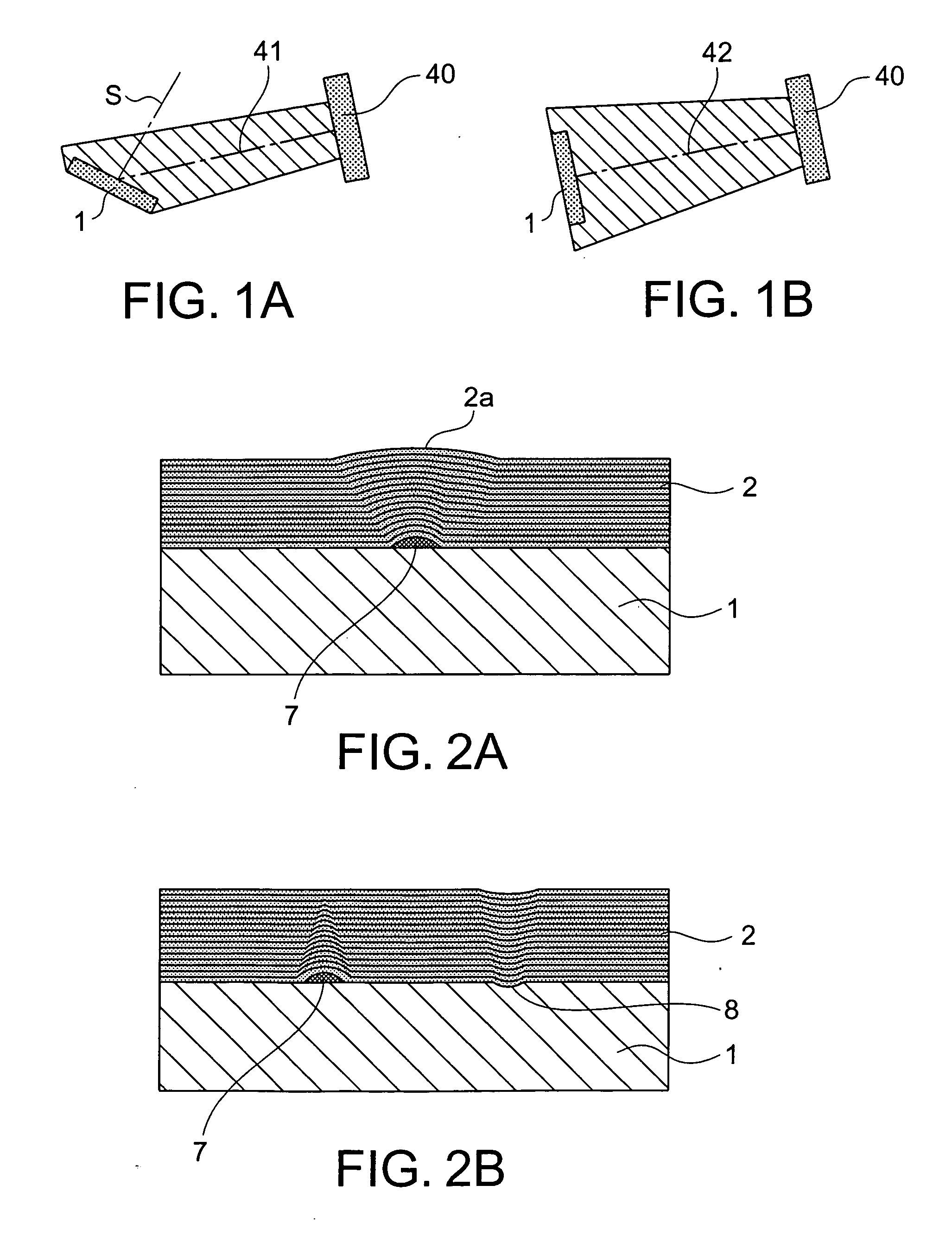
[0107] As a substrate, a low thermal expansion SiO2—TiO2-based glass substrate having a 152 mm square shape with a thickness of 6.35 mm was prepared. This glass substrate had a smooth surface of 0.15 nmRms and a flatness of 100 nm or less by mechanical polishing and cleaning.

[0108] Surface defects (convex and concave defects) on the surface of the obtained glass substrate were measured by the use of a defect inspection apparatus (MAGICS M-1350 manufactured by Lasertec Corporation). It was found that several hundreds of convex and concave defects were present over the entire substrate.

[0109] Then, a multilayer under film comprised of Mo / Si alternately-layered films was formed on the substrate. The film formation was carried out by the use of an ion beam sputtering apparatus. At first, the angle of the substrate in the apparatus was adjusted so that sputtered particles from a target were incident on the substrate from a direction inclined by 60° with respect to the perpendicular dir...

example 2

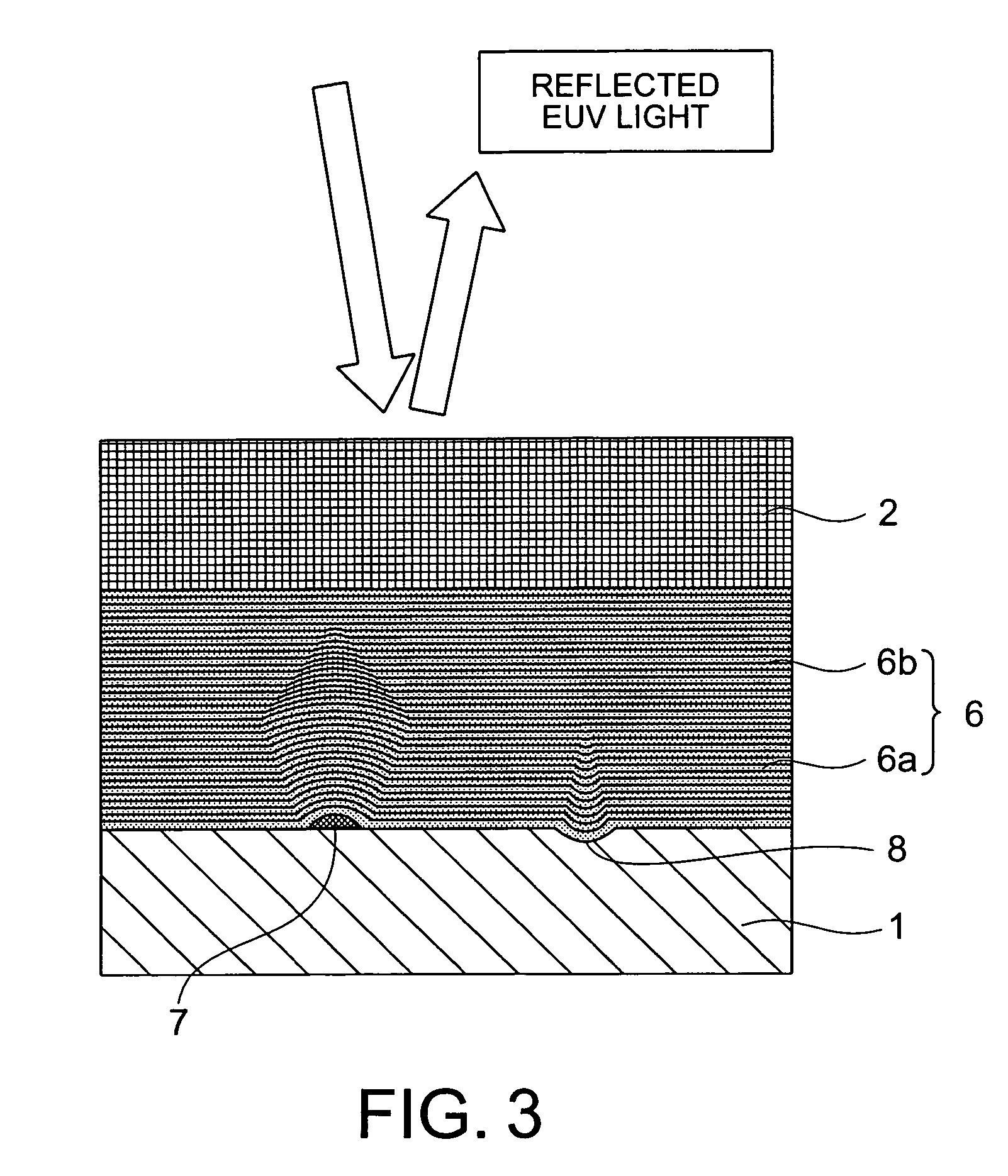
[0117] A multilayer reflective film coated substrate was produced in the same manner as in Example 1 except that a multilayer under film was formed such that the cycle length was 14.0 nm, ΓMo was 0.431, the number of cycles was 20, and the thickness was 280 nm, an intermediate layer was formed to a thickness of 14.0 nm, and a Si film and a RuNb film were formed to thicknesses of 4.0 nm and 2.5 nm, respectively, as a capping layer on the multilayer reflective film.

[0118] In this multilayer reflective film coated substrate, the relationship of the formula (1) can be satisfied when n=2 and the relationship of the formula (2) can be satisfied when m=2.

[0119] The reflectance of the multilayer reflective film of the multilayer reflective film coated substrate thus obtained was measured by applying EUV light of 13.5 nm at an incident angle of 6.0° and it was 64.7%.

[0120] Further, surface defects (convex and concave defects) of the multilayer reflective film were measured by the foregoin...

example 3

[0127] A buffer film made of chromium nitride (CrN: N=10 at %) was formed on the capping layer of the multilayer reflective film of the multilayer reflective film coated substrate obtained in Example 1. The film formation was carried out by the use of a DC magnetron sputtering apparatus and the thickness was set to 20 nm.

[0128] Then, a film containing Ta as a main component and further containing B and N was formed on the buffer film as an absorber film with respect to exposure light having a wavelength of 13 to 14 nm. The film formation was carried out in a DC magnetron sputtering apparatus using a target containing Ta and B and adding nitrogen in an amount of 10 vol % to argon. The thickness was set to 70 nm as a thickness that can sufficiently absorb the exposure light. The composition ratio of the formed TaBN film was such that Ta was 0.8, B was 0.1, and N was 0.1.

[0129] In the manner as described above, a reflective mask blank was produced.

[0130] Then, the absorber film of t...


PUM

PropertyMeasurementUnit
Thicknessaaaaaaaaaa

Abstract

A multilayer reflective film coated substrate includes a multilayer under film comprised of Mo/Si alternately-layered films, an intermediate layer in the form of a Si film, and a multilayer reflective film comprised of Mo/Si alternately-layered films for reflecting exposure light. The multilayer under film, the intermediate layer, and the multilayer reflective film are formed on a substrate in this order. Given that a cycle length of the multilayer under film is d bottom (unit:nm), a thickness of the intermediate layer is d Si (unit:nm), and a cycle length of the multilayer reflective film is d top (unit:nm), relationships of a formula (1) and a formula (2) are satisfied, the formula (1) given by
n×d top−0.05≦d bottom≦n×d top+0.05
where n is a natural number equal to or greater than 1, and the formula (2) given by
m×d top−1.2≦d Si≦−m×d top+1.2
where m is an integer equal to or greater than 0.

Description

[0001] This application claims priority to prior Japanese patent application JP2005-300575, the disclosure of which is incorporated herein by reference. BACKGROUND OF THE INVENTION [0002] This invention relates to a multilayer reflective film coated substrate, a manufacturing method thereof, a reflective mask blank, and a reflective mask. More specifically, this invention relates to a multilayer reflective film coated substrate having high surface smoothness with less defects which is suitable for a reflective mask for use in a lithography method using exposure light in a short wavelength region such as extreme ultraviolet light, and further relates to a method of efficiently manufacturing such a multilayer reflective film coated substrate, a reflective mask blank obtained using such a multilayer reflective film coated substrate, and a high-quality reflective mask obtained using such a reflective mask blank, which is less defective and excellent in pattern transferability. [0003] In...

Claims


Application Information

Patent Timeline
IPC IPC(8): F21V9/04C23C14/06C23C14/46G02B5/08G03F1/22G03F1/24G03F7/20G21K1/06H01L21/027
CPCB82Y10/00B82Y40/00C03C17/36C03C17/361C03C17/3636G03F1/24C23C14/185C23C14/225C23C14/3464G02B5/0833G02B5/0891C03C17/3665C03C17/3613C03C17/3615C03C17/3639C03C17/3649
Inventor HOSOYA, MARIOYAMADA, TAKEYUKIIKEDA, AKIRA
Owner HOYA CORP
Why Eureka
Try Eureka