
Number Of Pixels In Detector Arrays Using Compressive Sensing

Inactive Publication Date: 2013-03-21
BARANIUK RICHARD G +2
View PDF3 Cites 15 Cited by
  • Summary
  • Abstract
  • Description
  • Claims
  • Application Information

AI Technical Summary

Benefits of technology

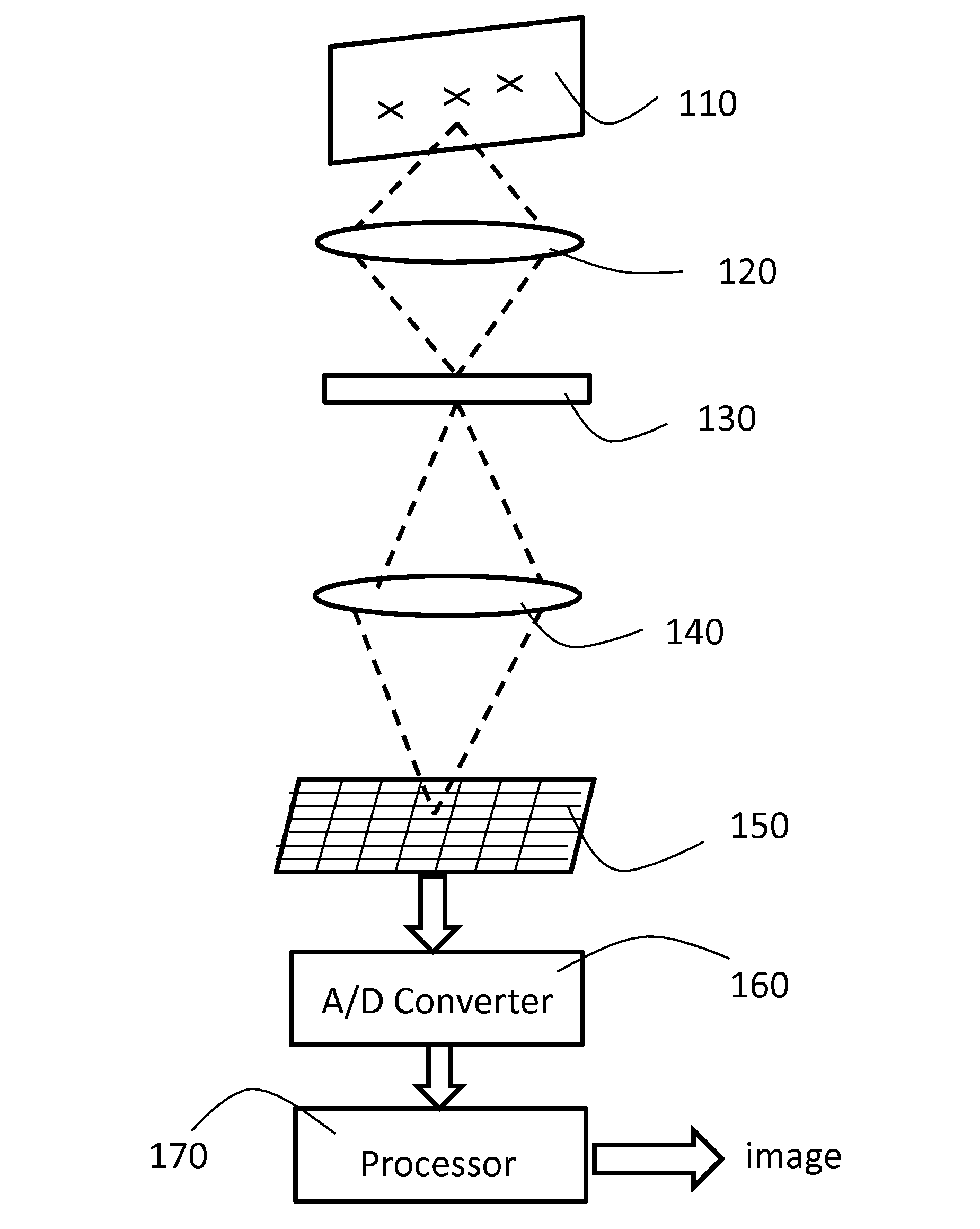
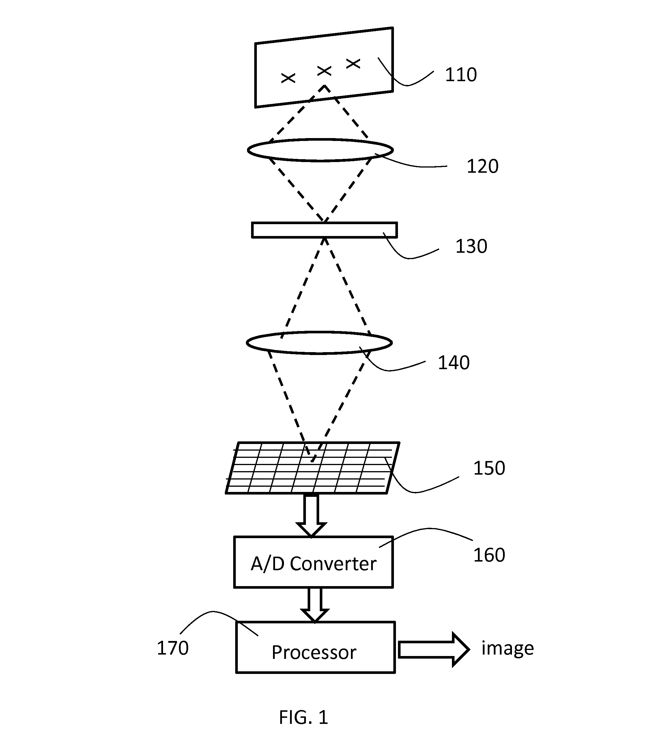
The present invention solves the problem of limited resolution in infrared imaging of semiconductor devices, and is applicable to any imaging situation where increased resolution is desired. It involves an image detector with a light focusing element, a spatial light modulator with P x N resolution elements, a re-imaging element, a P-pixel focal plane array detector, an A / D converter, and a processor. The processor recovers an image corresponding to an incident light field passing through the light focusing element using fewer than N times P measurements. The invention may also include a means for illuminating an object, a means for focusing light received at the image detector, means for modulating light received from the means for focusing light, a plurality of shadow masks in series or individually movable, a plurality of individually addressable photodiodes, or other variations. Overall, the invention allows for higher resolution imaging and improved analysis of semiconductor devices.

Problems solved by technology

Unfortunately, this requires a combinatorial search, which is prohibitively complex.

Method used


Image

  • Number Of Pixels In Detector Arrays Using Compressive Sensing
  • Number Of Pixels In Detector Arrays Using Compressive Sensing

Examples


Embodiment Construction

[0020]After fabrication, a large fraction of integrated circuits fail for various reasons. A key technique for finding the root cause of the failures is to analyze infrared images of the devices. Such devices contain hundreds of millions of transistors, each of which could emit light that points to the root cause. However, detector arrays currently available and those available in the foreseeable future have less than 1 Mpixel. Thus, one is forced to take multiple images of an integrated circuit (IC) at high magnification (and lower field of view) in order to precisely locate defect spots. The inventive technique disclosed here boosts the effective pixel count of the detector array by a factor of easily 10 and conceivably up to 104 or more. This would allow one to accomplish single-FOV imaging of an entire die in the semiconductor application space. Any image in which a pixel count significantly higher than the number of elements available in an array is required could benefit from ...


PUM


Abstract

A method and apparatus using the techniques of compressive sensing, which has so far been applied mostly to improving a single-pixel detector into an effectively N-pixel detector, for improving a P-pixel detector array into an effectively P×N-pixel detector array.

Description

CROSS-REFERENCE TO RELATED APPLICATIONS[0001]The present application claims the benefit of the filing date of U.S. Provisional Patent Application Ser. No. 61 / 306,824 entitled “Improved Pixel Counts in Detector Arrays Using Compressive Sensing” and filed by the present inventors on Feb. 22, 2010.[0002]The aforementioned provisional patent application is hereby incorporated by reference in its entirety.STATEMENT REGARDING FEDERALLY SPONSORED RESEARCH OR DEVELOPMENT[0003]None.BACKGROUND OF THE INVENTION[0004]1. Field of the Invention[0005]The invention relates to imaging devices such as cameras, video cameras, microscopes, and other visualization techniques, and more particularly, to methods and apparatus for improved number of pixels in detector arrays.[0006]2. Brief Description Of The Related Art[0007]A theory known as Compressive Sensing (CS) has emerged that offers both theory and practical strategies for directly acquiring a compressed digital representation of a signal without fi...

Claims


Application Information

Patent Timeline
IPC IPC(8): H04N5/378
CPCH04N5/378H04N5/335H04N25/00H04N25/78H04N25/75
Inventor BARANIUK, RICHARD GKELLY, KEVIN F.WOODS, GARY
Owner BARANIUK RICHARD G
Learn More