

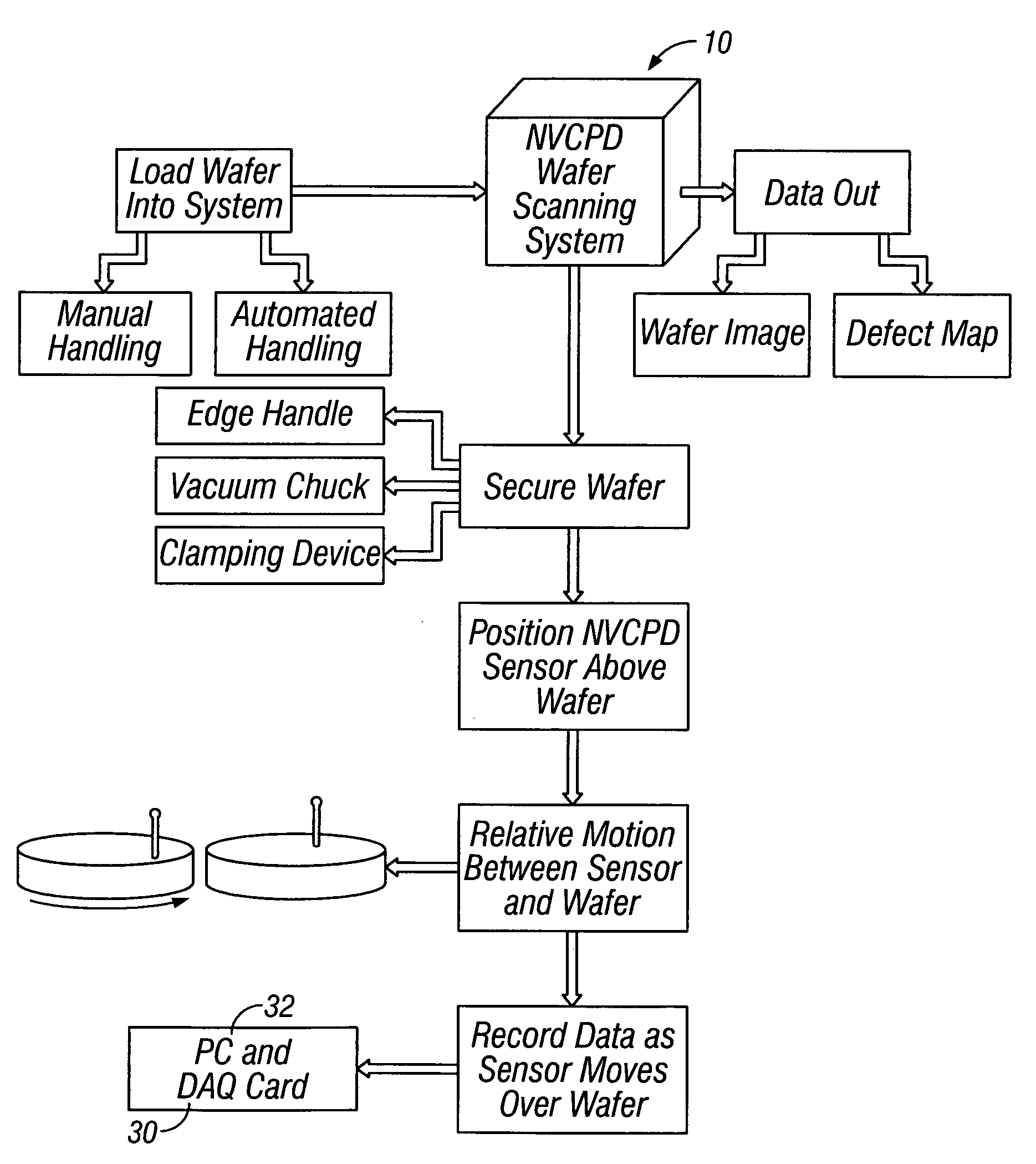
Inspection system and apparatus
a technology of inspection system and apparatus, applied in the direction of semiconductor/solid-state device testing/measurement, mechanical roughness/irregularity measurement, instruments, etc., can solve the problems of improper processing, processing equipment, poor handling technique, etc., to reduce the complexity of the sensor control mechanism, improve signal processing, and reduce processing costs.
- Summary
- Abstract
- Description
- Claims
- Application Information
AI Technical Summary
Benefits of technology
Problems solved by technology
Method used
Image

Examples
example 1
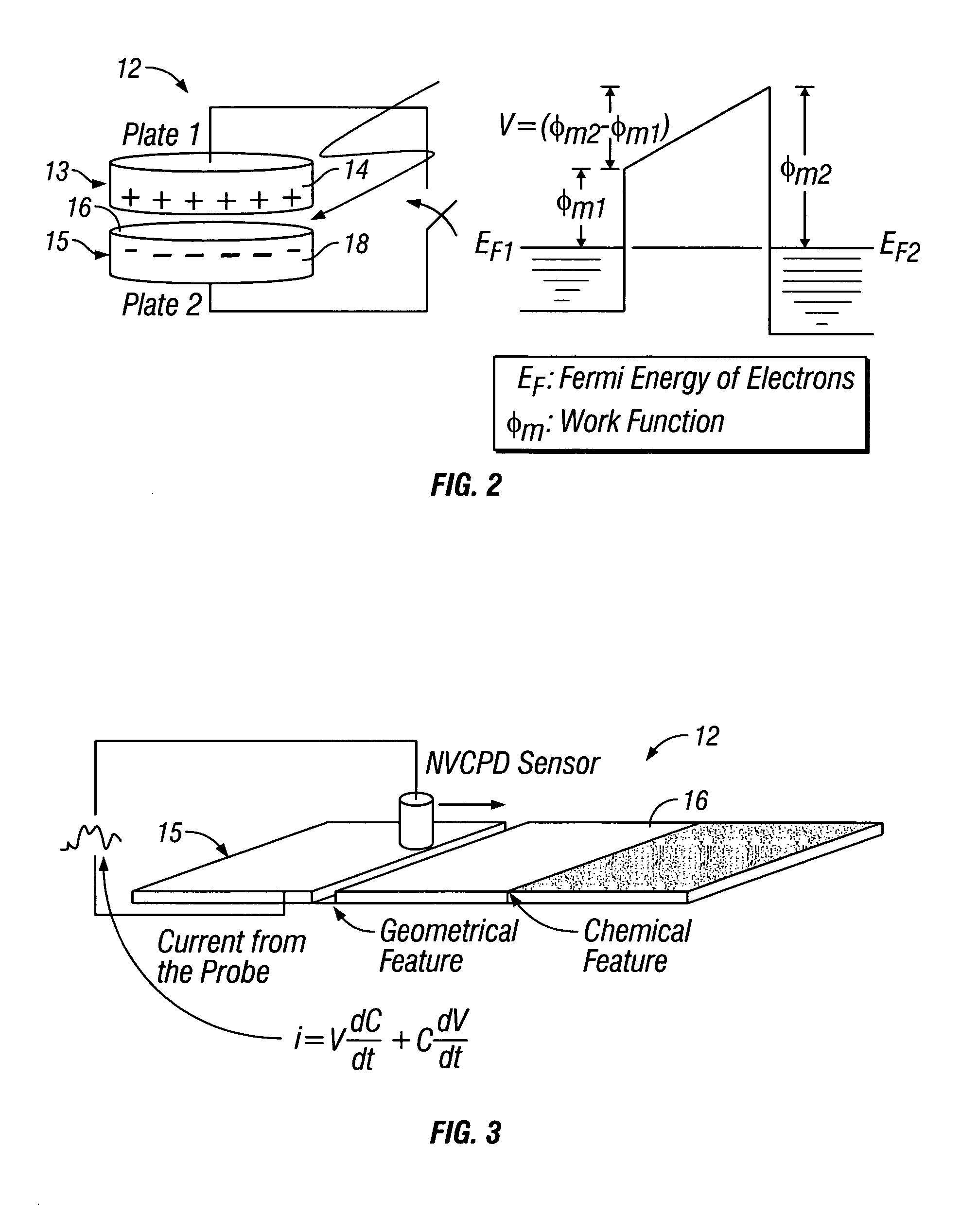
[0202]Sample wafers can be created by dip coating the wafer 15 in solutions that contain known concentrations of contaminants. Part of this example describes metal contaminants such as Cu and Fe, although any manner of chemical contaminants can be evaluated in this way. The wafer 15 described is either a 100 mm or 150 mm wafer, although these examples apply to any size wafer. The wafer surface 16 is prepared by dipping in HF to remove oxides. The wafer 15 is then cleaned and partially dipped in the metal contaminant solution. The amount of solution remaining on the wafer 15, and the resulting concentration of contaminant on the wafer surface 16, is controlled by selecting dip coating parameters such as the extraction rate.
[0203]Partial dipping of the test wafer 15 is preferred to create a transition from clean to contaminated areas. Because the nvCPD signal is differential, the nvCPD sensor 12 detects changes on the wafer surface 16, as opposed to an absolute value relating to surfa...
example 2
[0209]Measurements were made at six (6) locations on one hundred (100) millimeter wafer. The surface of the wafer was coated with gold on a first half. The second half was left uncoated, i.e. in its “natural”, bare silicon state. Three trials were performed on the bare silicon surface and the gold film surface. The probe—made from 500 micron diameter copper wire—was vibrated at 490 Hz, with a vibration amplitude of a few microns peak-to-peak. In addition, an ionizer was utilized to reduce the effect of surface charging. Ten measurements were made at each location. As can be seen in FIG. 32A, the nvCPD image produces a discernable image of the defect. However, as can be seen in FIG. 32B, the integrated image of the same differential nvCPD data produces a more distinct image of the defect. FIG. 33 is a graphical representation of the CPD data for each of the trials. In addition, FIG. 34A-B illustrates the precision of the present invention, showing the data for each of the ten measure...
example 3
[0210]In this example, different types of thin metal films were deposited on the same silicon substrate wafer to compare the nvCPD signal with the work function of materials. The wafer was divided into quadrants and each quadrant received unique deposition processing. Four different materials were deposited by DC sputtering on different quadrants of a silicon substrate through a shadow mask. The 1st quadrant (top right) was sputtered with copper, the 2nd quadrant (clockwise starting with number 1) was coated with chrome, the 3rd quadrant with titanium, and the 4th with aluminum. The sputtering time was set to achieve a film thickness of 100 angstroms in all quadrants.
[0211]The CPD image of the quadrant wafer is shown in FIG. 27. The lines and dots indicate the area where metal films are deposited. It can be seen that features in four quadrants are all detected by the nvCPD sensor, with different intensity and contrast. The CPD signal intensity can be extracted from a trackwise line ...
PUM
| Property | Measurement | Unit |
|---|---|---|
| thickness | aaaaa | aaaaa |
| diameter | aaaaa | aaaaa |
| relative dielectric constant | aaaaa | aaaaa |
Abstract
Description
Claims
Application Information