Delay circuit having reduced power supply voltage dependency

a delay circuit and power supply voltage technology, applied in the field of delay circuits, can solve the problems of excessive delay time, power supply voltage dependency of delay circuit time, and longer delay time, so as to reduce the power supply voltage dependency of delay time, delay time becomes shorter, and delay time is shorter

Inactive Publication Date: 2006-09-19
SOCIONEXT INC
View PDF13 Cites 15 Cited by
  • Summary
  • Abstract
  • Description
  • Claims
  • Application Information

AI Technical Summary

Benefits of technology

[0009]It is an object of the present invention to provide a delay circuit with reduced power supply voltage dependency.
[0011]According to the input signal, the first switch operates so that the capacitor is charged with the electric charge, and the second switch operates so that the electric charge is discharged from the capacitor. When the capacitor is charged with, for example, a power supply voltage, the time required for discharging the electric charge from the capacitor is longer as the power supply voltage is higher. Since this discharge time corresponds to the delay time, such a characteristic is exhibited that the delay time becomes longer as the power supply voltage is higher. Conversely, the comparison circuit has a characteristic such that its delay time becomes shorter as the power supply voltage is higher. Consequently, the delay characteristics of the both are cancelled out by each other, so that it is possible to reduce the power supply voltage dependency of the delay time.

Problems solved by technology

The delay time of the delay circuit has power supply voltage dependency.
The lowered power supply voltage causes the delay time to be longer.
In a case where the restore time is set in a delay circuit using a high power supply voltage, the use of a low-power supply voltage results in an excessively long delay time if the power supply voltage dependency of the delay time is too large.
The excessively long delay time results in an excessively long access time of the RAM determined by the low power supply voltage.

Method used


Image

  • Delay circuit having reduced power supply voltage dependency
  • Delay circuit having reduced power supply voltage dependency
  • Delay circuit having reduced power supply voltage dependency

Examples


Embodiment Construction

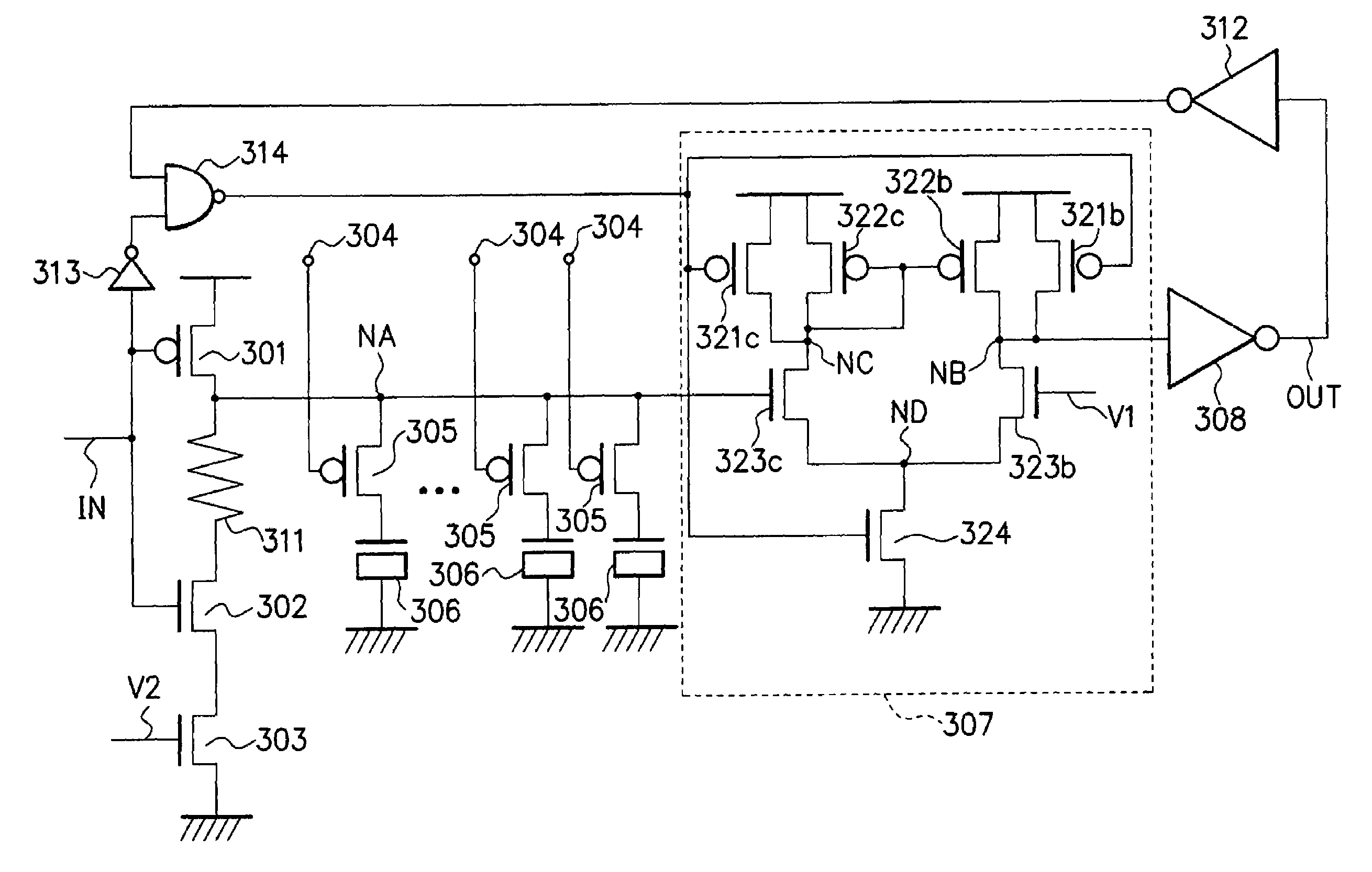
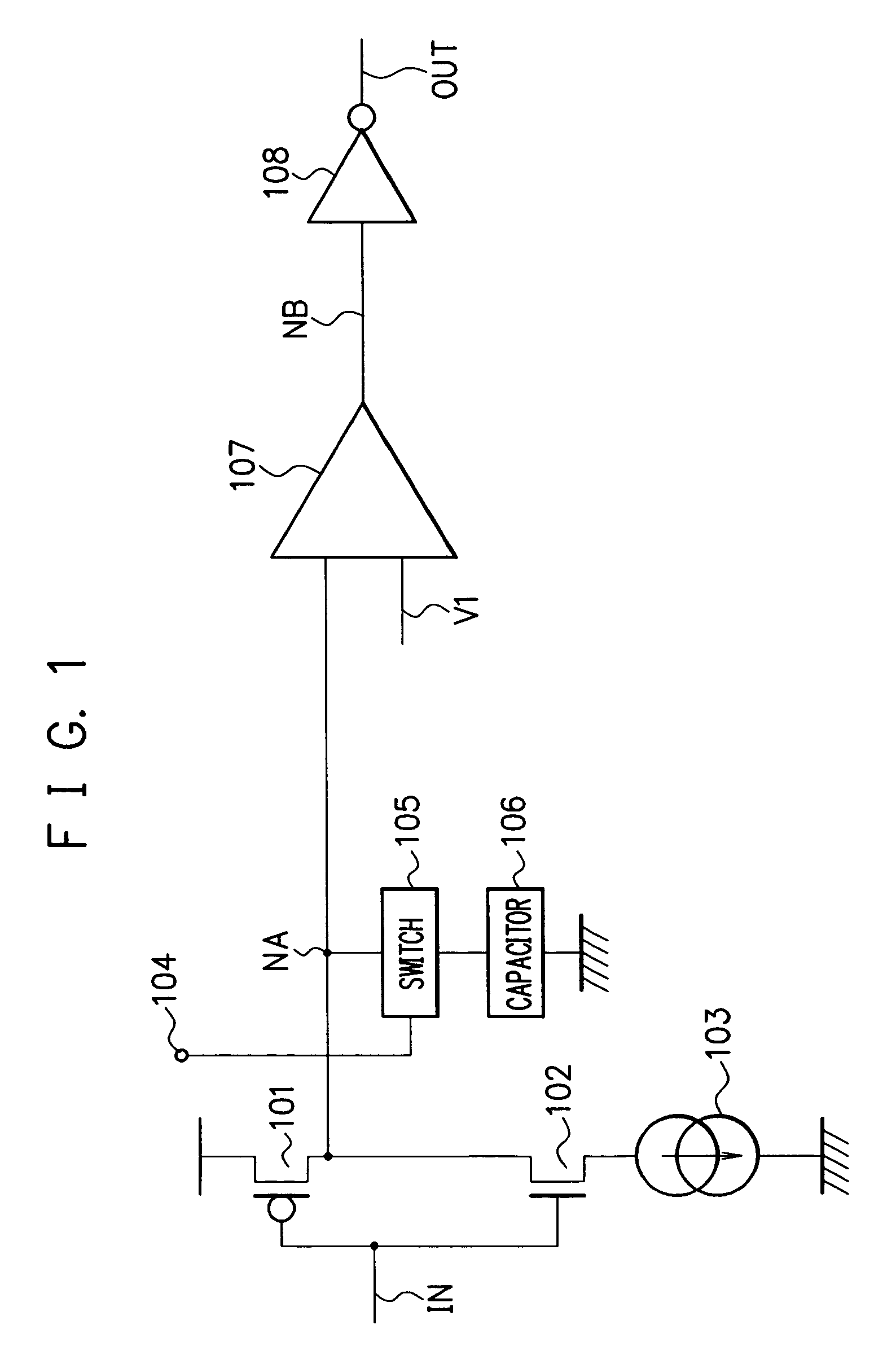
[0021]FIG. 1 shows a configuration example of a delay circuit according to an embodiment of the present invention. An input signal line IN is a line through which an input signal is inputted. A p-channel MOS transistor 101 has a gate connected to the input signal line IN, a source connected to a power supply potential, and a drain connected to a node NA. An n-channel MOS transistor 102 has a gate connected to the input signal line IN and a drain connected to the node NA. A constant current source (constant current circuit) 103 is connected between a source of the transistor 102 and a ground potential. Since the transistors 101 and 102 constitute an inverter, a logic inverted signal of the input signal of the input signal line IN appears at the node NA.

[0022]Series connection of a switch 105 and a capacitor 106 is connected between the node NA and the ground potential. When a switch control signal is inputted to a terminal 104, the switch 105 is controlled to turn on or off, so that ...


PUM


Abstract

A delay circuit includes: an input signal line (IN) through which an input signal is inputted; a capacitor (106) charged with and discharging electric charge; a first switch (101) connected to the input signal line and operating according to the input signal when the capacitor is to be charged with electric charge; a second switch (102) connected to the input signal line and operating according to the input signal when the electric charge is to be discharged from the capacitor; and a comparison circuit (107) comparing a voltage of the capacitor and a reference voltage to output a delay signal of the input signal.

Description

[0001]This nonprovisional application is a continuation application of and claims the benefit of International Application No. PCT / JP03 / 05931 filed May 13, 2003. The disclosure of the prior application is hereby incorporated herein in its entirety by reference.TECHNICAL FIELD[0002]The present invention relates to a delay circuit, and more particularly, to a delay circuit having a capacitor.BACKGROUND ART[0003]FIG. 9 shows a configuration of a delay circuit according to a conventional art. An input signal line IN is connected to gates of a p-channel MOS transistor 901 and an n-channel MOS transistor 902. A source of the transistor 901 is connected to a power supply potential, and a source of the transistor 902 is connected to a ground potential. A resistor 903 is connected between drains of the transistors 901 and 902. They constitute a first-stage inverter.[0004]An output of the first-stage inverter is the drain of the transistor 901, which is connected to an input signal line of a ...

Claims


Application Information

Patent Timeline
Patent Type & Authority Patents(United States)
IPC IPC(8): H03H11/26H03K5/00H03K5/13
CPCG11C7/22G11C7/222G11C11/406G11C11/40615G11C11/4076G11C29/023G11C29/028H03H11/265H03K5/133G11C29/02H03K2005/00071
Inventor TOMITA, HIROYOSHI
Owner SOCIONEXT INC
Why Eureka
Try Eureka