Capacitance detection apparatus, driving method for the same, fingerprint sensor, and biometric authentication apparatus

a capacitive detection and driving method technology, applied in the field of capacitive detecting technology for reading, can solve the problems of high cost of forming sensors from single-crystal silicon substrates, unstable potential of data lines, and broken sensors, and achieve high precision and stable sensing.

Active Publication Date: 2006-10-24
138 EAST LCD ADVANCEMENTS LTD
View PDF16 Cites 12 Cited by
  • Summary
  • Abstract
  • Description
  • Claims
  • Application Information

AI Technical Summary

Benefits of technology

[0006]An aspect of the invention can provide a capacitance detection apparatus, a fingerprint sensor, and a biometric authentication apparatus that solve the above problems and make highly precise and stable sensing possible. Further the invention to provide a method that can carry out sensing of capacitance with high precision.

Problems solved by technology

However, since related capacitance-type fingerprint sensors are formed on single-crystal silicon substrates, there has been the problem of the sensors breaking when firmly pressed with the fingertip of the user.
Since a fingerprint sensor needs to be constructed in a size approximately equal to the area (around 20 mm by 20 mm) of a fingertip, there has also been the problem of high cost when forming sensors from single-crystal silicon substrates.
In addition, in a construction where capacitance detection circuits that are combinations of sensor electrodes and transistors are disposed in a matrix, if the data lines that are the signal transmitting paths are respectively connected to a plurality of capacitance detection circuits, when the information of the capacitance detection circuits inside the matrix is read, the output information of the capacitance detection circuits in the same column but on previous rows remains and the initial potential of the data lines is not stable, so that there has been the problem that stable sensing has not been possible.

Method used


Image

  • Capacitance detection apparatus, driving method for the same, fingerprint sensor, and biometric authentication apparatus
  • Capacitance detection apparatus, driving method for the same, fingerprint sensor, and biometric authentication apparatus
  • Capacitance detection apparatus, driving method for the same, fingerprint sensor, and biometric authentication apparatus

Examples


Embodiment Construction

[0023]A first exemplary embodiment of the invention will now be described with reference to the drawings.

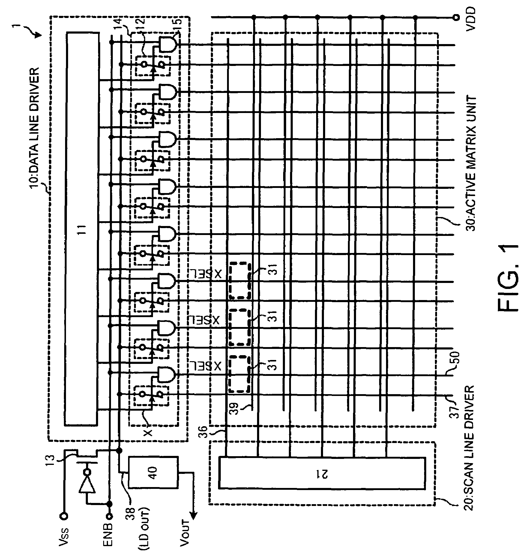
[0024]FIG. 1 is an exemplary block diagram showing a capacitance-type fingerprint sensor 1 that is a capacitance detection apparatus according to the invention. As shown in FIG. 1, the fingerprint sensor 1 can include a data line driver 10 for selecting data lines 37 that are signal transmitting paths, a scan line driver 20 for selecting scan lines 36, an active matrix unit 30 that functions as a fingerprint detection unit, and an amplification circuit 40 for amplifying detection signals. The data line driver 10 can include a shift register 11 that decides the timing at which the data lines 37 are successively selected and a reset period selecting circuit 14 that sets a reset period. The reset period selecting circuit 14 includes analog switches 12, which connect and disconnect the respective data lines 37 and a global data line 38, and logical AND circuits 15, which take a logic...


PUM


Abstract

Aspects of the invention can provide a fingerprint sensor with high sensing precision. The fingerprint sensor according to the invention can include capacitance detection circuits that output detection signals, which each correspond to a capacitance formed between a subject surface and the fingerprint sensor, to signal transmitting paths, and an amplification circuit that amplifies the detection signals outputted to the signal transmitting paths. The individual signal transmitting paths can be respectively connected to at least two capacitance detection circuits and the fingerprint sensor further includes a resetting means that resets the potential of the signal transmitting paths before the detection signals are outputted from the capacitance detection circuits to the signal transmitting paths.

Description

BACKGROUND OF THE INVENTION[0001]1. Field of Invention[0002]Aspects of the invention relate to a capacitance detecting technology for reading, as variations in capacitance, the surface form of a subject, such as a fingerprint, that has minute convexes and concaves.[0003]2. Description of Related Art[0004]Japanese Unexamined Patent Publication Nos. H11-118415, 2000-346608, 2001-56204, and 2001-133213 disclose a related technology where the surface of a sensor electrode formed on a single-crystal silicon substrate is covered with a dielectric film, the potential of a fingertip is set as a reference potential, and variations in the capacitance formed between a fingertip and sensor electrodes due to the convexes and concaves of the fingerprint are used to identify the fingerprint.SUMMARY OF THE INVENTION[0005]However, since related capacitance-type fingerprint sensors are formed on single-crystal silicon substrates, there has been the problem of the sensors breaking when firmly pressed ...

Claims


Application Information

Patent Timeline
Patent Type & Authority Patents(United States)
IPC IPC(8): G01R27/26G01B7/28A61B5/117G06K9/00G06T1/00
CPCG06K9/0002G06V40/1306
Inventor HARA, HIROYUKI
Owner 138 EAST LCD ADVANCEMENTS LTD
Why Eureka
Try Eureka