

Multi-power ring chip scale package for system level integration
a scale package and multi-power ring chip technology, applied in the direction of semiconductor devices, semiconductor/solid-state device details, electrical apparatus, etc., can solve the problems of exaggerated difficulties, difficulty in reconciling, and the number of chronic difficulties of the electronics industry
- Summary
- Abstract
- Description
- Claims
- Application Information
AI Technical Summary
Problems solved by technology
Method used
Image

Examples
embodiment 100
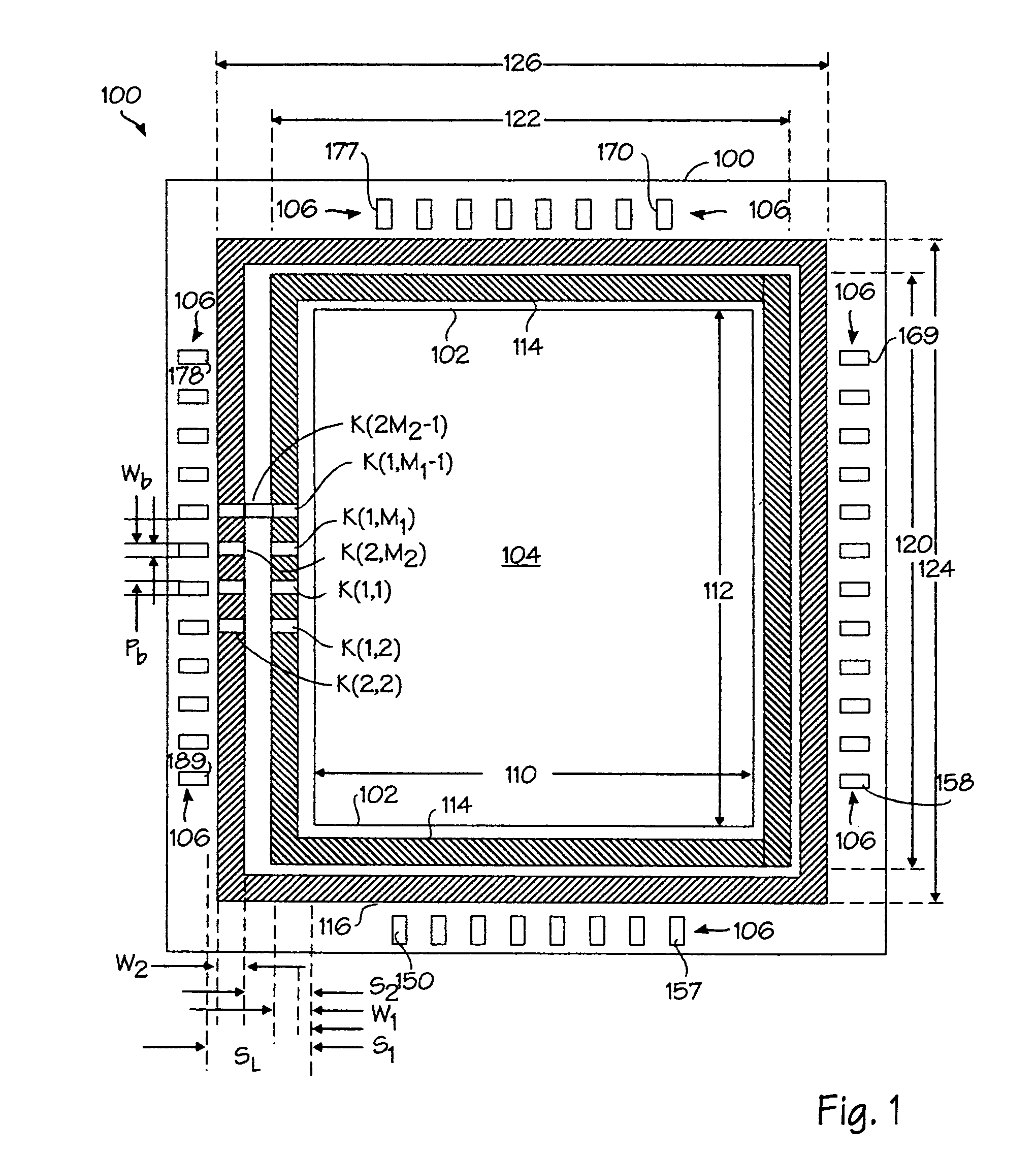
[0045]With reference to FIG. 1, there is shown a plan view of the interior of an embodiment 100 of the present multi-power ring IC package invention indicated by the arrow enumerated as 100. External package electrodes (e.g. package pins, bumps or solder balls) for routing from selected external PC board electrode patterns to internal package bonding electrodes are not shown. Such routing and external electrode lead formation and placement is known in the art and assumed to be present in permissible number, form and location appropriate for a particular size, external lead type and package aspect ratio of embodiments of the present invention. For example, the multi-power ring package 100 can be considered to be a Ball-Grid-Array (BGA) type package having an appropriate permissible number and location of solder balls such as those shown as balls 54 in FIG. 3 in the referenced U.S. Pat. No. '545 by Schueller.
[0046]One of the most significant issues for any IC package type and size is ...
embodiment 300
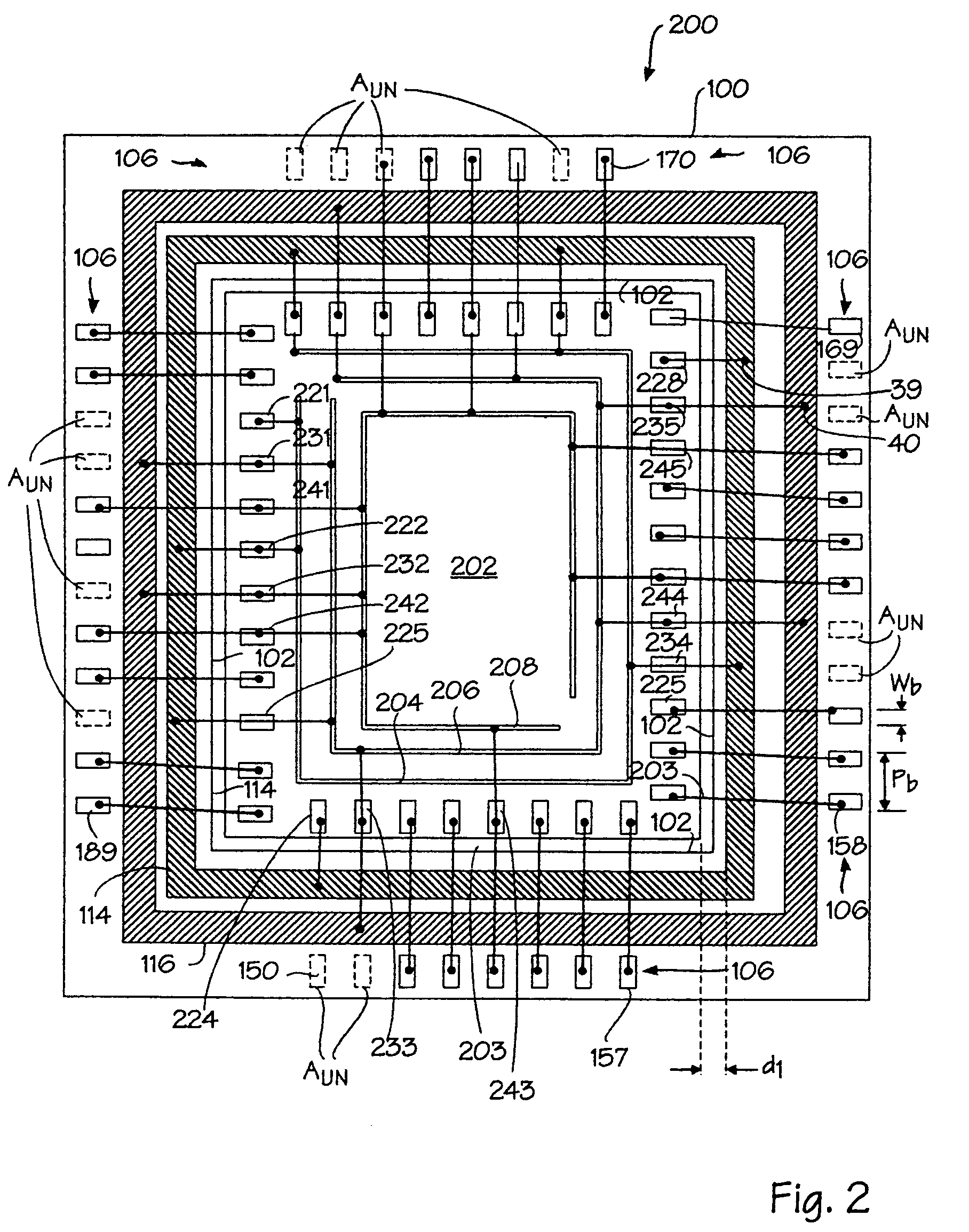
[0069]Referring now to FIG. 3 and FIG. 4 there are shown alternative embodiments of multi-power ring IC packages according to the present invention. FIG. 3 is a segmented annular power ring embodiment 300 of the present invention showing four annular power ring segments 302, 304, 306 and 308. Segments 302 and 304 are respective opposed C-shaped segments formed by separating the complete annular power ring 114 of FIG. 2 into the two electrically isolated pieces 302 and 304 defining insulating voids 312. Segments 306 and 308 are opposed C-shaped segments formed by separating the complete annular power ring 116 of FIG. 1 into the two electrically isolated pieces 306 and 308 defining insulating voids 310.
[0070]The segments 302, 304, 306 and 308 of FIG. 3 would enable mounting and bonding a multi-power IC chip having 4 independent power supply nets, each net bonded separately by respective power-net bonding pads to a separate-one of the four isolated power ring segments. Four appropriate...
PUM
 Abstract
Description
Claims
Application Information