
Superconducting latch driver circuit generating sufficient output voltage and pulse-width

a superconducting latch and driver circuit technology, applied in the direction of pulse technique, instruments, code conversion, etc., can solve the problems of reducing the operating margin of the sfq circuit, and it is difficult to drive signal lines with large characteristic impedance directly at high speed, so as to reduce ground ripples and facilitate output a plurality

Inactive Publication Date: 2006-10-31
FUJITSU LTD +1
View PDF8 Cites 20 Cited by
  • Summary
  • Abstract
  • Description
  • Claims
  • Application Information

AI Technical Summary

Benefits of technology

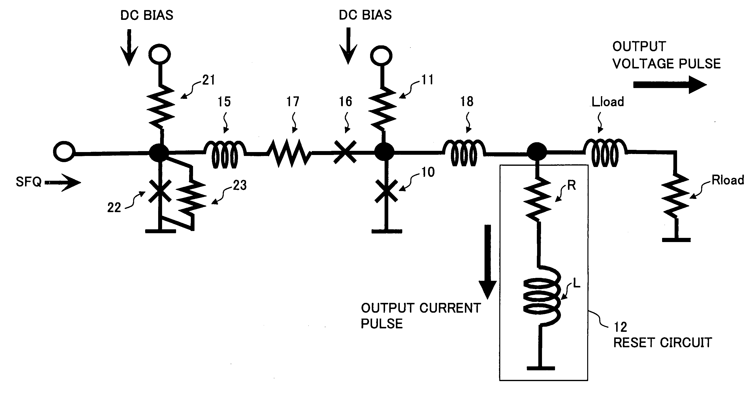
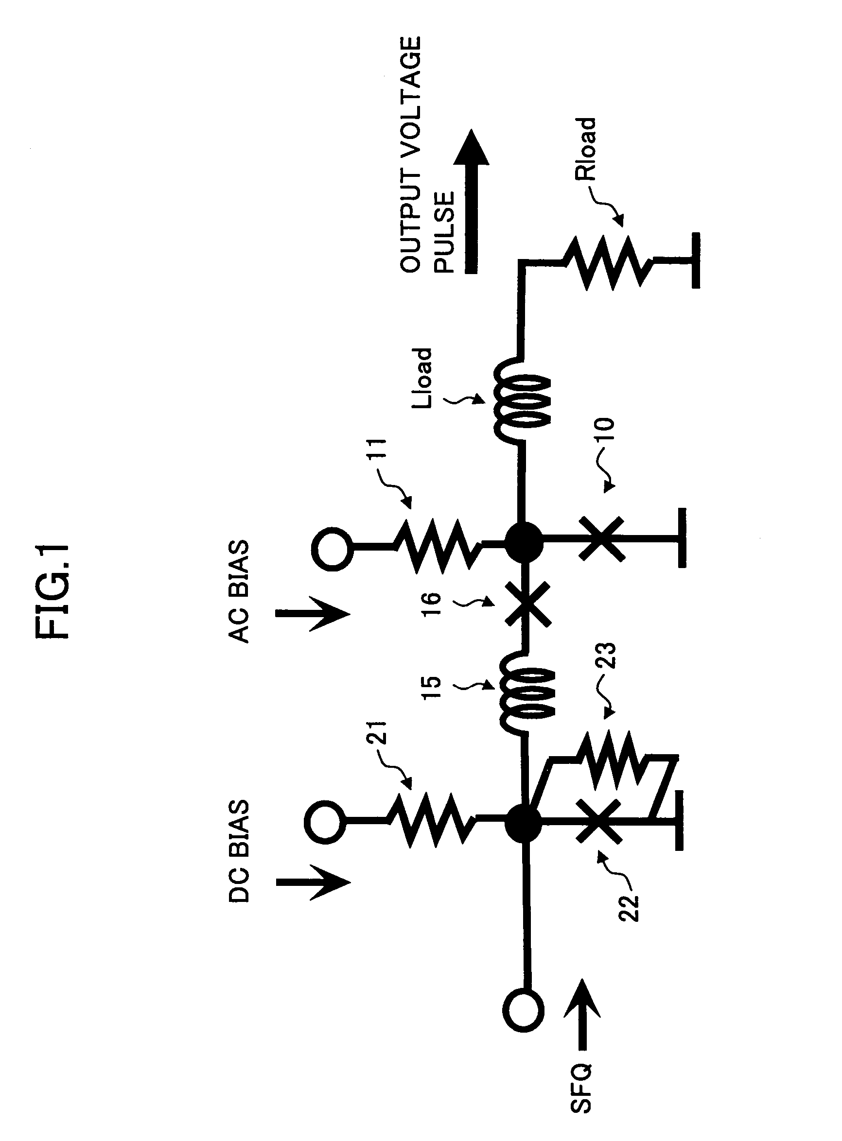
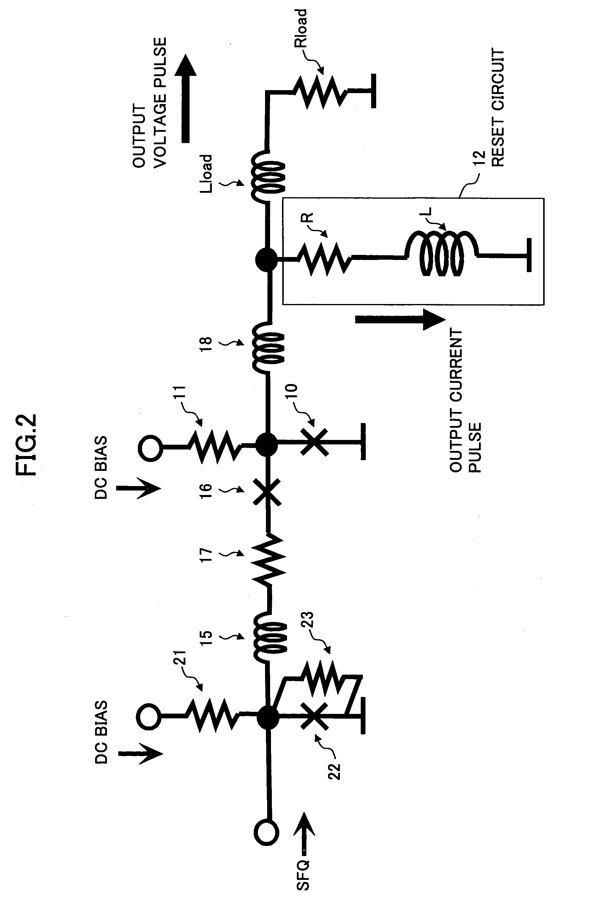
[0019]According to at least one embodiment of the invention, a voltage pulse on the order of millivolts is output by use of only a direct-current bias, thereby making it possible to reduce ground ripples. It thus becomes easier to output a plurality of data items in parallel using a plurality of interface circuits. An output of the reset circuit can also be used as an electric-current pulse output. With the high drive capability and the self-reset function, the latch driver circuit of the invention may be used as a feedback driver for a superconducting double-loop sigma-delta modulator. Further, because it is possible to drive a high-resistance load of about 100Ω, the latch driver circuit of the invention may be used not only as an output interface for an SFQ circuit but also for data transmission between SFQ circuits in a multi-chip module (MCM).

Problems solved by technology

This AC bias current, however, may generate the fluctuation of ground potential, which results in the operating margin of the SFQ circuit being reduced, or ends up being mixed into an input signal.
Because an output voltage of these circuits is as small as in the range of hundreds micro bolts, however, it is difficult to drive signal lines having large characteristic impedance directly at high speed.

Method used


Image

  • Superconducting latch driver circuit generating sufficient output voltage and pulse-width
  • Superconducting latch driver circuit generating sufficient output voltage and pulse-width
  • Superconducting latch driver circuit generating sufficient output voltage and pulse-width

Examples


first embodiment

[0106]FIG. 13 is an illustrative drawing showing the superconducting SFQ circuit according to the second aspect of the invention. In FIG. 13, the same elements as those of FIG. 12 are referred to by the same numerals, and a description thereof will be omitted.

[0107]In FIG. 13, a chip 110A, which is a superconducting SFQ circuit according to the invention, includes a superconducting circuit 111A, a superconducting circuit 112A, and n stages of superconducting SFQ circuits 113A-1 through 113A-n. The superconducting SFQ circuits 113A-1 through 113A-n connect between the superconducting circuit 111A and the superconducting circuit 112A. Couplings to the biases and the ground are the same as in the construction shown in FIG. 12. The superconducting circuit 111A includes a superconducting SFQ circuit 131 and a ground plane 133-1, and the superconducting circuit 112A includes a superconducting SFQ circuit 132 such as an output circuit and a ground plane 133-2. The illustrated circuit confi...

second embodiment

[0110]FIG. 14 is an illustrative drawing showing the superconducting SFQ circuit according to the second aspect of the invention. In FIG. 14, the same elements as those of FIG. 13 are referred to by the same numbers, and a description thereof will be omitted.

[0111]In FIG. 14, a chip 110B, which is a superconducting SFQ circuit according to the invention, includes the superconducting circuit 111A, the superconducting circuit 112A, and the n stages of superconducting SFQ circuits 113A-1 through 113A-n. The superconducting SFQ circuits 113A-1 through 113A-n make up a Josephson transmission line (JTL) The superconducting SFQ circuit 113A-x (x=1, 2, . . . , n) includes the ground plane 115-x, the inductance 116-x, the Josephson junction 117-x, the Josephson junction 118-x, and the inductances LUx and LLx that provide connections with adjoining circuits.

[0112]The higher the frequency, the greater the impedance of inductance becomes. Even if the ground potential of the superconducting circ...

third embodiment

[0115]FIG. 15 is an illustrative drawing showing the superconducting SFQ circuit according to the second aspect of the invention. In FIG. 15, the same elements as those of FIG. 14 are referred to by the same numbers, and a description thereof will be omitted.

[0116]In FIG. 15, a chip 110C, which is a superconducting SFQ circuit according to the invention, includes the superconducting circuit 111A, a superconducting circuit 112C, and the n stages of superconducting SFQ circuits 113A-1 through 113A-n. The superconducting SFQ circuits 113A-1 through 113A-n make up a Josephson transmission line. The superconducting SFQ circuit 113A-x (x=1, 2, . . . , n) includes the ground plane 115-x, the inductance 116-x, the Josephson junction 117-x, the Josephson junction 118-x, and the inductances LUx and LLx that provide connections with adjoining circuits. A resistance Rx is provided on the DC+ side and a resistance RGx is provided on the DC− side of the superconducting SFQ circuit 113A-x. Such re...


PUM


Abstract

A circuit includes a latch circuit including a Josephson junction and configured to perform a latch operation based on a hysteresis characteristic in response to a single flux quantum, a load circuit including load inductance and load resistance and coupled to an output of the latch circuit, and a reset circuit provided between the output of the latch circuit and the load circuit and configured to reset the latch circuit a predetermined time after the latch operation by the latch circuit, wherein the Josephson junction is driven by a direct current.

Description

CROSS-REFERENCE TO RELATED APPLICATIONS[0001]The present application is based upon and claims the benefit of priority from the prior Japanese Patent Application No. 2003-305959 filed on Aug. 29, 2003, Japanese Patent Application No. 2004-066100 filed on Mar. 9, 2004, and Japanese Patent Application No. 2004-066101 filed on Mar. 9, 2004, with the Japanese Patent Office, the entire contents of which are incorporated herein by reference.BACKGROUND OF THE INVENTION[0002]1. Field of the Invention[0003]The present invention generally relates to superconducting latch driver circuits, and particularly relates to a superconducting latch driver circuit driven with a DC bias current.[0004]2. Description of the Related Art[0005]As a macroscopic quantum effect of a superconductor, a loop formed by the superconductor results in magnetic flux being quantized within the loop. The magnetic flux that is quantized in the superconductor is called an SFQ (single flux quantum). An SFQ circuit is a logic ...

Claims


Application Information

Patent Timeline
Patent Type & Authority Patents(United States)
IPC IPC(8): H03M1/00H03K3/38H03M3/02
CPCH03K3/38H03M3/438H03M3/43
Inventor HIRANO, SATORUSUZUKI, HIDEOTANABE, KEIICHIYOSHIDA, AKIRAHATO, TSUNEHIROMARUYAMA, MICHITAKA
Owner FUJITSU LTD
Learn More