Method for creating a self-aligned SOI diode by removing a polysilicon gate during processing

a polysilicon gate and soi diode technology, applied in the field of integrated circuit technologies, can solve the problems of gate oxide breakdown limitation, gate oxide breakdown, increased capacitance loading, etc., and achieve the effect of reducing the capacitance loading of the diod

a polysilicon gate and soi diode technology, applied in the field of integrated circuit technologies, can solve the problems of gate oxide breakdown limitation, gate oxide breakdown, increased capacitance loading, etc., and achieve the effect of reducing the capacitance loading of the diod

US7138313B2Inactive Publication Date: 2006-11-21INT BUSINESS MASCH CORP

Image

  • Method for creating a self-aligned SOI diode by removing a polysilicon gate during processing
  • Method for creating a self-aligned SOI diode by removing a polysilicon gate during processing
  • Method for creating a self-aligned SOI diode by removing a polysilicon gate during processing

Examples


Embodiment Construction

[0029]The invention and the various features and advantageous details thereof are explained more fully with reference to the non-limiting embodiments that are illustrated in the accompanying drawings and detailed in the following description. It should be noted that the features illustrated in the drawings are not necessarily drawn to scale. Descriptions of well-known components and processing techniques are omitted so as to not unnecessarily obscure the invention. The examples used herein are intended merely to facilitate an understanding of ways in which the invention may be practiced and to further enable those of skill in the art to practice the invention. Accordingly, the examples should not be construed as limiting the scope of the invention.

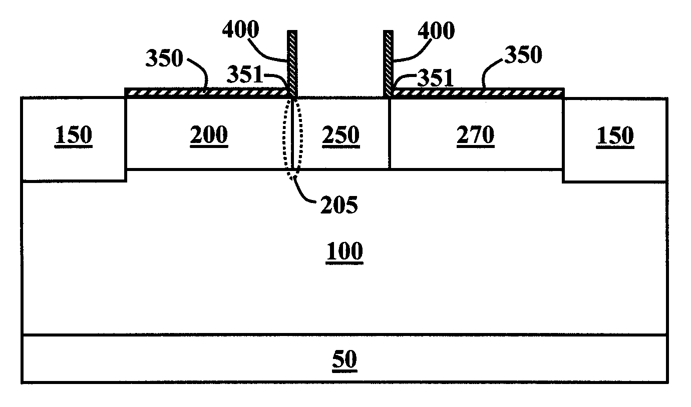
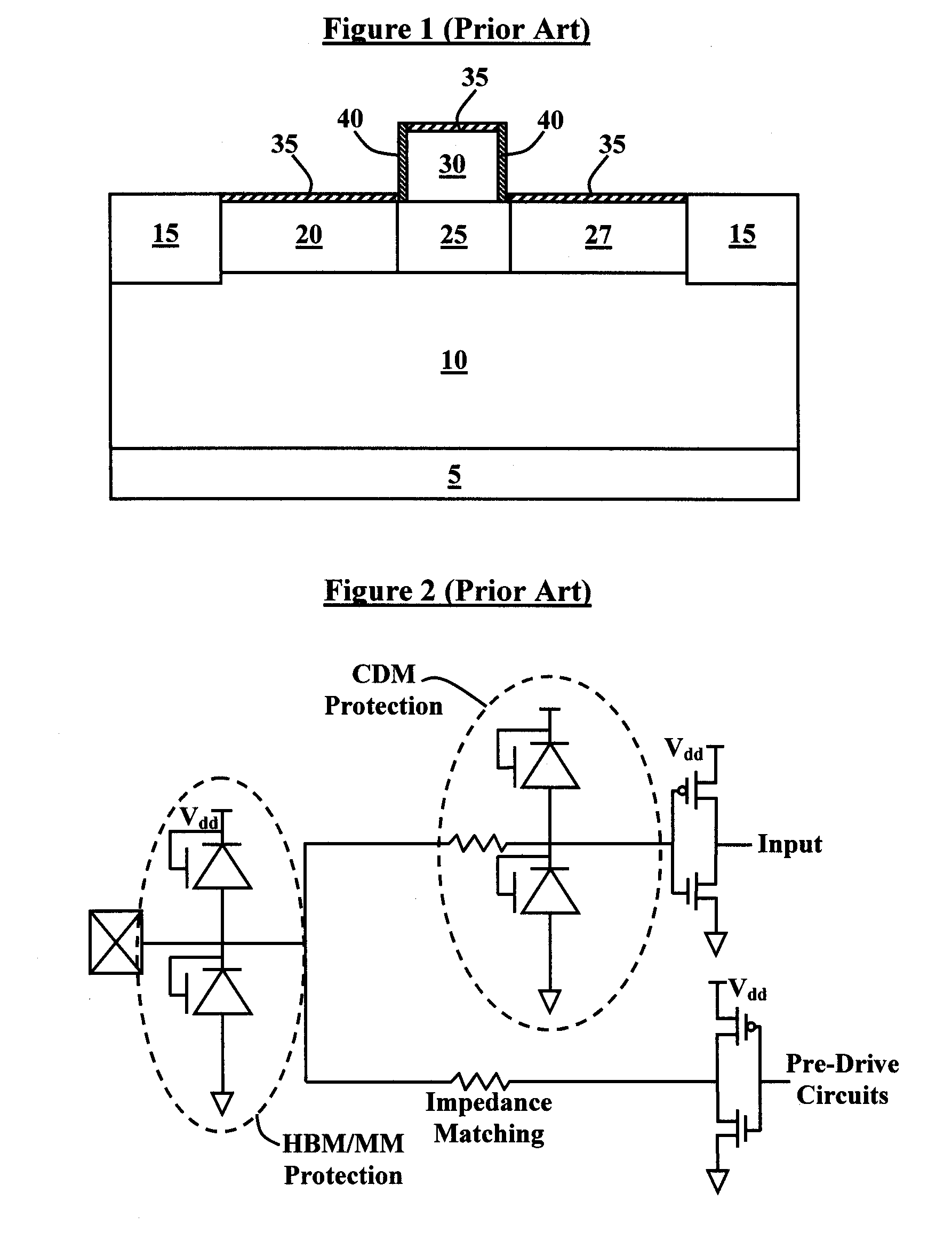
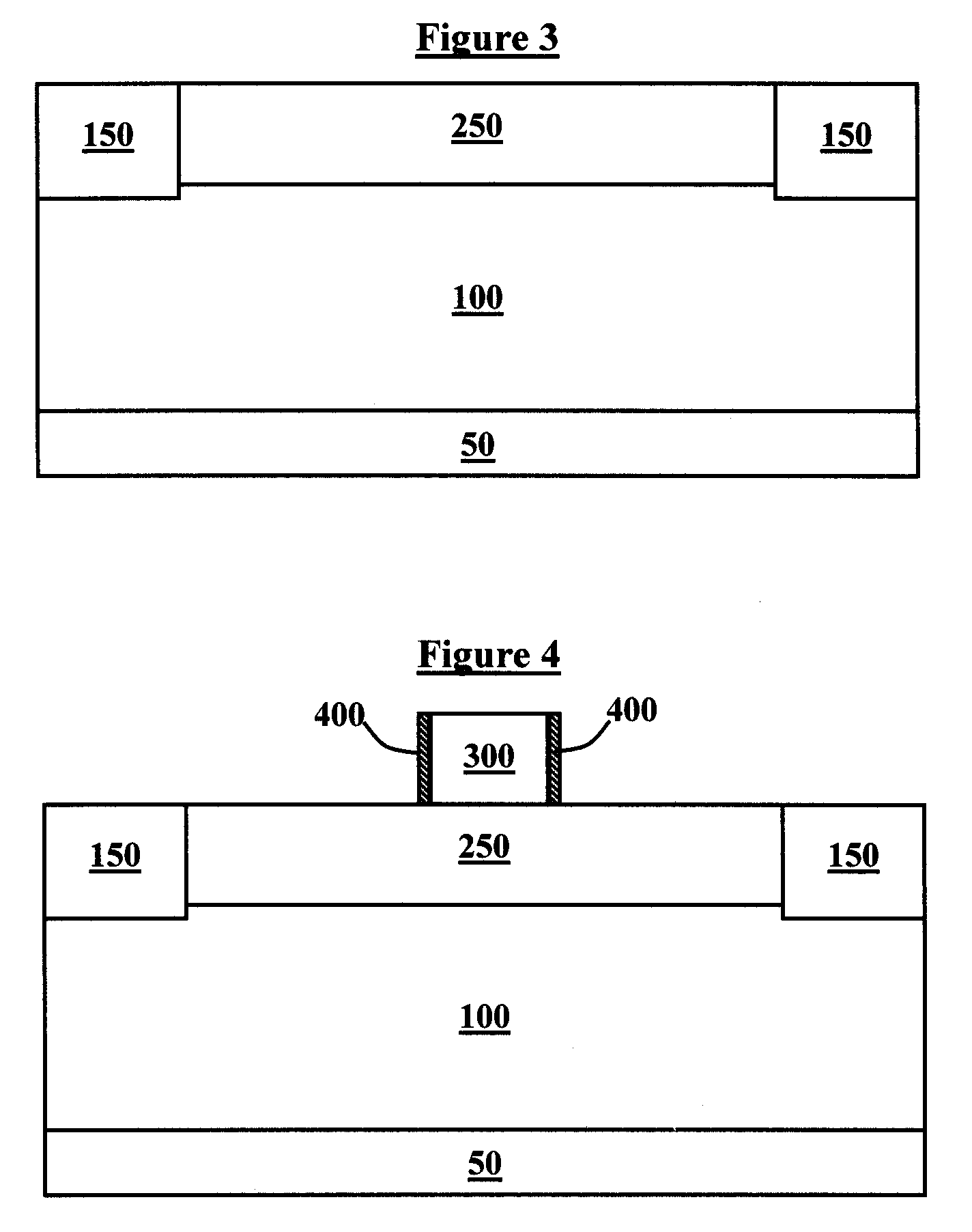
[0030]As previously mentioned, there is a need for a novel method for processing a self-aligned low capacitance SOI ESD diode, which does not include a polysilicon gate in the final diode structure. Referring now to the drawings, and more ...


PUM


Abstract

A method of forming a self-aligned SOI diode, the method comprising depositing a protective structure over a substrate; implanting a plurality of diffusion regions of variable dopant types in an area between at least one pair of isolation regions in the substrate, the plurality of diffusion regions separated by a diode junction, wherein the implanting aligns an upper surface of the diode junction with the protective structure; and removing the protective structure. The method further comprises forming a silicide layer over the diffusion regions and aligned with the protective structure. The protective structure comprises a hard mask, wherein the hard mask comprises a silicon nitride layer. Alternatively, the protective structure comprises a polysilicon gate and insulating spacers on opposite sides of the gate. Furthermore, in the removing step, the spacers remain on the substrate.

Description

BACKGROUND OF INVENTION[0001]1. Field of the Invention[0002]The invention generally relates to integrated circuit technologies, and more particularly to silicon on insulator, electrostatic discharge diodes incorporated in field effect transistor structures.[0003]2. Description of the Related Art[0004]Conventionally, diodes offered in silicon on insulator (SOI) technologies require the use of polysilicon to serve as a self-aligning mask for the anode / cathode and to block silicide formation, preventing shorting between the anode and cathode regions of the device. The standard practice is for the polysilicon gate to remain after processing is completed. However, this approach has two disadvantages; gate oxide breakdown limitations and increased capacitance loading.[0005]An example of a conventional diode structure is illustrated in FIG. 1, wherein the diode is formed on a single area of silicon over a buried oxide insulator 10 over a substrate 5, and in between the shallow trench isola...

Claims


Application Information

Patent Timeline
21 Nov 2006
Publication
US7138313B2
IPC
H01L21/8234; H01L21/329; H01L21/84; H01L27/02; H01L27/12; H01L29/861
CPC
H01L27/0255; H01L29/66136; H01L29/861; H01L21/84; H01L27/1203
Inventors
CHATTY, KIRAN V.; GAUTHIER, JR., ROBERT J.