Shift register and display device and driving method thereof

a shift register and display device technology, applied in semiconductor devices, digital storage, instruments, etc., can solve the problems of power consumption of clock signals inputted to the driver circuit, the gate width of a tft included in the driver circuit needs to be increased, and the signal decreases or increases the same amount as the threshold voltage of the tft, so as to reduce the load caused by clock signals and reduce the power consumption of the shift register.

Active Publication Date: 2013-09-03
SEMICON ENERGY LAB CO LTD
View PDF152 Cites 12 Cited by
  • Summary
  • Abstract
  • Description
  • Claims
  • Application Information

AI Technical Summary

Benefits of technology

[0012]In view of the above problems, an object of one embodiment of the present invention is to reduce the power consumption of a shift register or a display device including the shift register.
[0013]The above problems can be solved by dividing a clock signal line included in a shift register into a plurality of pulse signal lines. In other words, a plurality of flip-flops included in the shift register is not electrically connected to one clock signal line; and a plurality of pulse signal lines is provided and part of the plurality of flip-flops is electrically connected to one of the plurality of pulse signal lines. The pulse signal line supplies a clock signal in part of an operation period of the shift register, not during the whole operation period of the shift register. Therefore, the capacity load caused with the supply of clock signals to the shift register can be reduced, leading to reduction in power consumption of the shift register.
[0020]In a shift register which is one embodiment of the present invention, a clock signal is supplied by a plurality of wirings, not by one wiring. Any one of the plurality of wirings supplies a clock signal in only part of the operation period of the shift register, not during the whole operation period of the shift register. Therefore, the capacity load caused with the supply of clock signals can be reduced, leading to reduction in power consumption of the shift register.

Problems solved by technology

For example, in the case where the shift register includes only unipolar TFTs, there is a problem in that a signal decreases or increases by the same amount as the threshold voltage of the TFT.
Therefore, bootstrap operation is often performed in a portion where such a problem occurs.
Further, in the case where the load of a driver circuit utilizing bootstrap is heavy, a gate width of a TFT included in the driver circuit needs to be made larger.
As a result, there is a problem in that the power consumption of a clock signal inputted to the driver circuit is made large by the parasitic capacitance.

Method used


Image

  • Shift register and display device and driving method thereof
  • Shift register and display device and driving method thereof
  • Shift register and display device and driving method thereof

Examples


embodiment 1

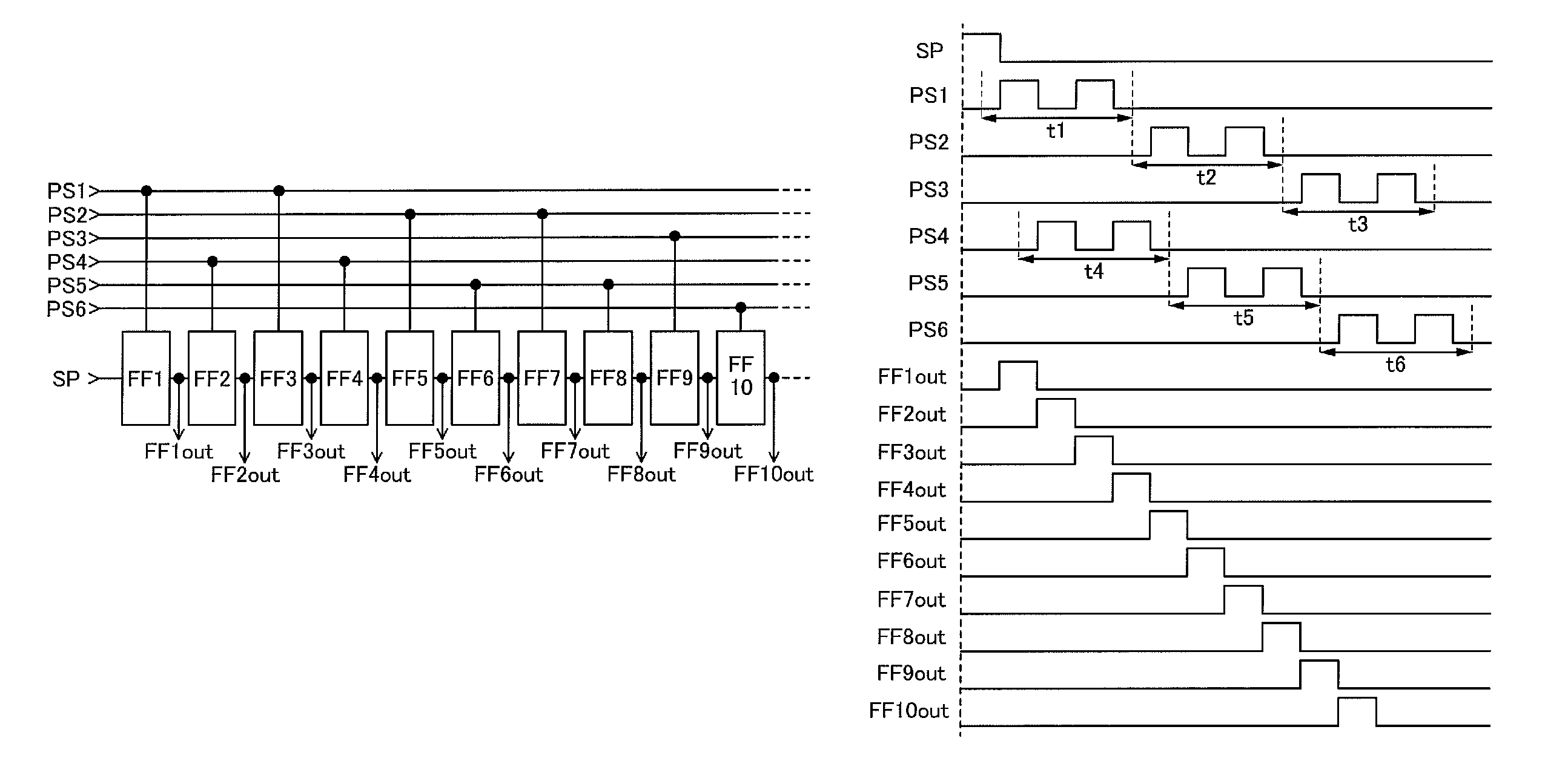
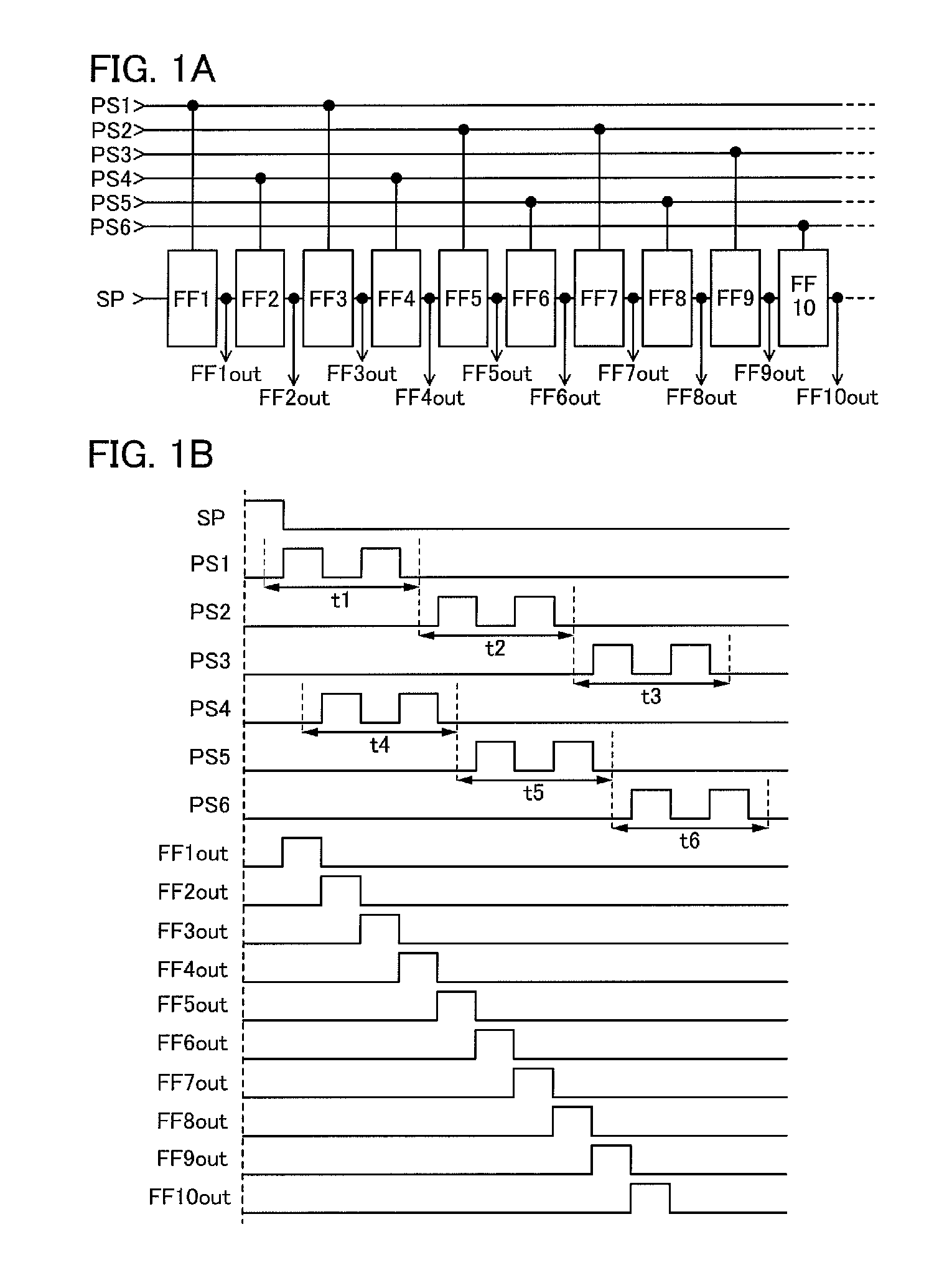
[0047]In this embodiment, examples of a structure and operation of a shift register are described with reference to FIGS. 1A and 1B, FIGS. 2A and 2B, FIGS. 3A and 3B, FIGS. 4A and 4B, FIGS. 5A to 5C, FIGS. 6A to 6C, and FIGS. 7A and 7B. Specifically, a shift register which includes a pulse signal line and a flip-flop is described. The pulse signal line serves as a wiring for supplying a clock signal in part of the operation period of the shift register and serves as a wiring for supplying a low power supply potential in the other periods. The flip-flop is electrically connected to the pulse signal line.

[0048]A shift register in this embodiment includes first to sixth pulse signal lines and first to tenth flip-flops.

[0049]The first pulse signal line (PS1) is electrically connected to the first flip-flop (FF1) and the third flip-flop (FF3). The second pulse signal line (PS2) is electrically connected to the fifth flip-flop (FF5) and the seventh flip-flop (FF7). The third pulse signal ...

embodiment 2

[0110]In this embodiment, an example of a transistor which is applicable to the shift register described in Embodiment 1 will be described.

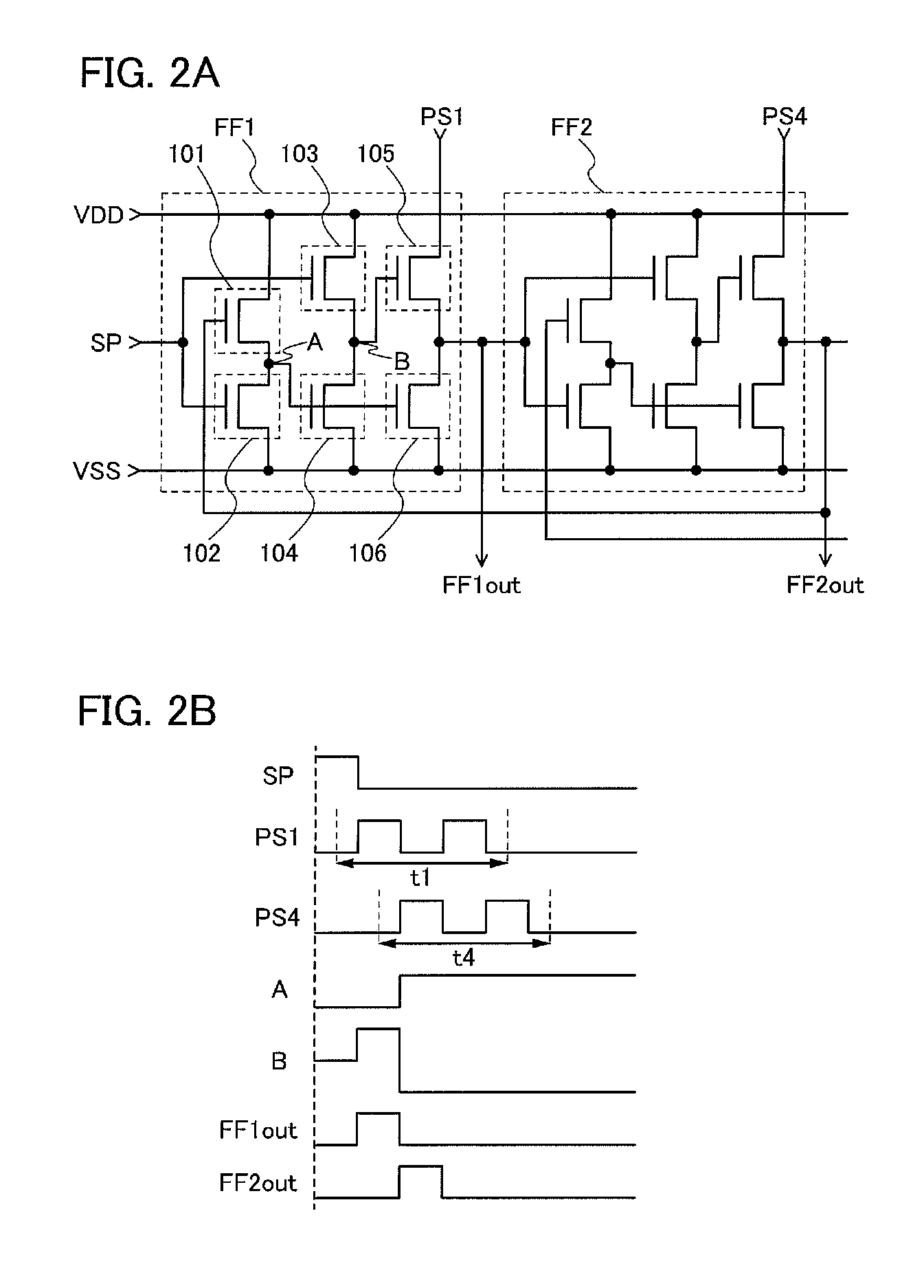
[0111]Examples of structures of the transistors of this embodiment will be described with reference to FIGS. 8A to 8C. FIGS. 8A to 8C illustrate examples of the structures of the transistors of this embodiment. FIG. 8A is a top diagram and FIG. 8B is a cross-sectional diagram taken along line Z1-Z2 in FIG. 8A.

[0112]The transistor in FIGS. 8A and 8B includes a conductive layer 211 over a substrate 201, an insulating layer 202 over the conductive layer 211, an oxide semiconductor layer 213 over the insulating layer 202, and a conductive layer 215a and a conductive layer 215b over the oxide semiconductor layer 213.

[0113]Note that in the transistor, the conductive layer 211 serves as a gate terminal, the insulating layer 202 serves as a gate insulating layer, one of the conductive layers 215a and 215b serves as a source terminal, and the other of the...

embodiment 3

[0181]In this embodiment, another example of a transistor which is applicable to the shift register described in Embodiment 1 and different from the transistor described in Embodiment 2 will be described.

[0182]An example of a structure of the transistor of this embodiment will be described with reference to FIGS. 12A and 12B. FIGS. 12A and 12B illustrate an example of a structure of the transistor of this embodiment. FIG. 12A is a top diagram of the transistor and FIG. 12B is a cross-sectional diagram taken along line Z1-Z2 in FIG. 12A.

[0183]The transistor illustrated in FIGS. 12A and 12B includes the conductive layer 211 over the substrate 201; the insulating layer 202 over the conductive layer 211; the conductive layers 215a and 215b over the insulating layer 202; the oxide semiconductor layer 213 over the insulating layer 202 and the conductive layers 215a and 215b.

[0184]In the transistor, the conductive layer 211 serves as a gate terminal, the insulating layer 202 serves as a g...


PUM


Abstract

The power consumption of a shift register or a display device including the shift register is reduced. A clock signal is supplied to a shift register by a plurality of wirings, not by one wiring. Any one of the plurality of wirings supplies a clock signal in only part of the operation period of the shift register, not during the whole operation period of the shift register. Therefore, the capacity load caused with the supply of clock signals can be reduced, leading to reduction in power consumption of the shift register.

Description

TECHNICAL FIELD[0001]The present invention relates to a shift register and a display device including the shift register.BACKGROUND ART[0002]A thin film transistor (TFT) formed over a flat plate such as a glass substrate, which is typically used in a liquid crystal display device, is generally formed using a semiconductor material such as amorphous silicon or polycrystalline silicon. Although a TFT which is formed using amorphous silicon has low field-effect mobility, such a TFT can be formed over a larger glass substrate. On the other hand, a TFT formed using polycrystalline silicon has high field-effect mobility, but such a TFT needs a crystallization step such as laser annealing and is not always suitable for being formed over a larger glass substrate.[0003]In view of the foregoing, a TFT formed using an oxide semiconductor as a semiconductor material has attracted attention. For example, Patent Documents 1 and 2 each disclose a technique in which a TFT is formed using zinc oxide...

Claims


Application Information

Patent Timeline
Patent Type & Authority Patents(United States)
IPC IPC(8): G11C19/00
CPCG09G3/3266G09G3/3677G11C19/28H01L27/1225G09G2300/0408G09G2300/0417G09G2310/0267G09G2330/021G09G3/3208G09G3/36G09G2310/0286G09G3/20G11C19/00
Inventor KOYAMA, JUN
Owner SEMICON ENERGY LAB CO LTD
Why Eureka
Try Eureka