Thin film transistor array substrate, manufacturing method and liquid crystal display panel

A technology of thin film transistors and array substrates, applied in the field of liquid crystal display, capable of solving problems such as affecting the driving capability of thin film transistors 14, affecting the display effect of the screen, and large signal delay, so as to improve the display effect of the screen, reduce the layout area, and reduce the capacitive load. Effect

Active Publication Date: 2017-03-08
KUSN INFOVISION OPTOELECTRONICS
View PDF13 Cites 12 Cited by
  • Summary
  • Abstract
  • Description
  • Claims
  • Application Information

AI Technical Summary

Problems solved by technology

[0006] In the existing technology, the distance between the data line 12 and the scanning line 11 and between the data line 12 and the storage capacitor line 13 is determined by the first insulating layer 16. In order to reduce the capacitive load of the data line 12, it can be considered to increase the first insulating layer 16. The thickness of the first insulating layer 16, but because the data line 12 and the source electrode 142 and the drain electrode 143 of the thin film transistor 14 are in the same layer, increasing the thickness of the first insulating layer 16 will affect the driving capability of the thin film transistor 14 at the same time
Therefore, the capacitive load of the data line 12 in the prior art is relatively large, resulting in a large signal delay, which cannot achieve the purpose of reducing power consumption and affects the display effect of the screen.

Method used


Image

  • Thin film transistor array substrate, manufacturing method and liquid crystal display panel
  • Thin film transistor array substrate, manufacturing method and liquid crystal display panel
  • Thin film transistor array substrate, manufacturing method and liquid crystal display panel

Examples


no. 1 example

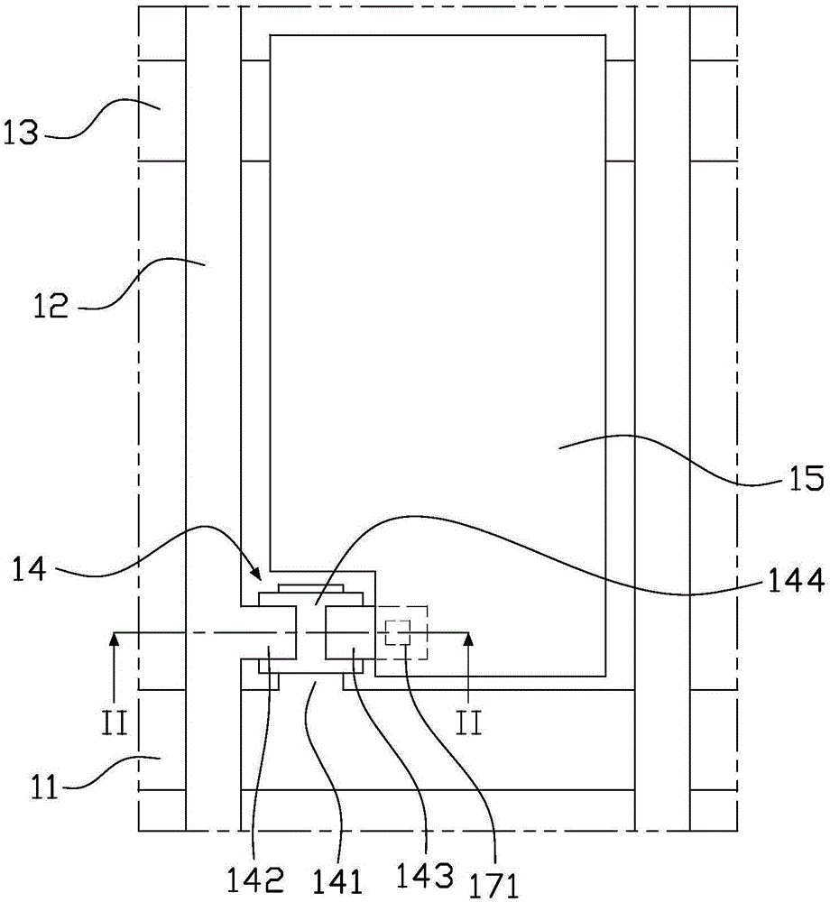
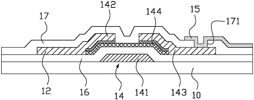
[0047] image 3 is a partial schematic diagram of the thin film transistor array substrate in the first embodiment of the present invention, Figure 4 for image 3 Schematic cross-section along the IV-IV direction, such as Figure 3-4 As shown, the thin film transistor array substrate provided in this embodiment includes a substrate 10, a first metal layer formed on the substrate 10, a first insulating layer 16 covering the first metal layer, and a first insulating layer 16 formed on the first insulating layer 16. The active layer 144 on the top, the second metal layer formed on the first insulating layer 16, the second insulating layer 17 covering the second metal layer, the third metal layer formed on the second insulating layer 17, covering The third insulating layer 18 on the third metal layer, and the pixel electrode 15 formed on the third insulating layer 18 .

[0048] The first metal layer includes scan lines 11 and gates 141 ; the second metal layer includes source ...

no. 2 example

[0071] Figure 7 It is a schematic cross-sectional view of a thin film transistor array substrate in the second embodiment of the present invention. The structure and manufacturing method of this embodiment are basically the same as those of the above-mentioned first embodiment. The fourth insulating layer 19 of 15, and the common electrode 20 (common electrode) is fabricated on the fourth insulating layer 19, so that the above-mentioned array substrate can be used as an array substrate of a fringe field switching mode (Fringe Field Switching, FFS) liquid crystal display panel.

no. 3 example

[0073] Figure 8 It is a schematic cross-sectional view of the thin film transistor array substrate in the third embodiment of the present invention. The structure and manufacturing method of this embodiment are basically the same as those of the first embodiment above. A common electrode 20 (common electrode) is formed on the layer 18, wherein the pixel electrode 15 and the common electrode 20 are comb-shaped structures and are inserted into each other in the same layer, so that the above-mentioned array substrate can be used as an in-plane switch mode (In-Plane Switch , IPS) the array substrate of the liquid crystal display panel.


PUM


Abstract

Provided are a thin film transistor array substrate, a manufacturing method and a liquid crystal display panel. The thin film transistor array substrate comprises a substrate, a first metal layer, a first insulation layer, an active layer, a second metal layer, a second insulation layer, a third metal layer, a third insulation layer and a pixel electrode. The first metal layer is formed on the substrate and comprises a scanning line and a grid. The first metal layer is covered with the first insulation layer, and the active layer is formed on the first insulation layer. The second metal layer is formed on the first insulation layer and comprises a source electrode and a drain electrode. The second metal layer is covered with the second insulation layer, and a first contact hole and a second contact hole are formed in the second insulation layer. The third metal layer is formed on the second insulation layer and comprises a data line and a conductive block, the data line is connected with the source electrode through the first contact hole, and the conductive block is connected with the drain electrode through the second contact hole. The third metal layer is covered with the third insulation layer, and a third contact hole is formed in the third insulation layer. The pixel electrode is formed on the third insulation layer, and the pixel electrode is connected with the conductive block through the third contact hole.

Description

technical field [0001] The invention relates to the technical field of liquid crystal display, in particular to a thin film transistor array substrate, a manufacturing method and a liquid crystal display panel. Background technique [0002] With the development of display technology, liquid crystal display panels (Liquid Crystal Display, LCD) are more and more popular due to their advantages of lightness and low radiation. The liquid crystal display panel includes an opposite color filter substrate (color filter, CF) and a thin film transistor array substrate (TFT array), and a liquid crystal layer (LC layer) sandwiched between them. [0003] figure 1 is a partial schematic diagram of a thin film transistor array substrate in the prior art, figure 2 for figure 1 Schematic cross-section along II-II direction, such as Figure 1-2 As shown, the thin film transistor array substrate includes scanning lines 11, data lines 12 and storage capacitor lines 13, and a plurality of ...

Claims


Application Information

Patent Timeline
Patent Type & Authority Applications(China)
IPC IPC(8): G02F1/1362H01L27/12H01L21/77
CPCH01L27/124H01L27/1259G02F1/136213G02F1/136227
Inventor 徐芸刘飒
Owner KUSN INFOVISION OPTOELECTRONICS
Why Eureka
Try Eureka