Driving circuit and display device
- Summary
- Abstract
- Description
- Claims
- Application Information
AI Technical Summary
Benefits of technology
Problems solved by technology
Method used
Image

Examples
first embodiment
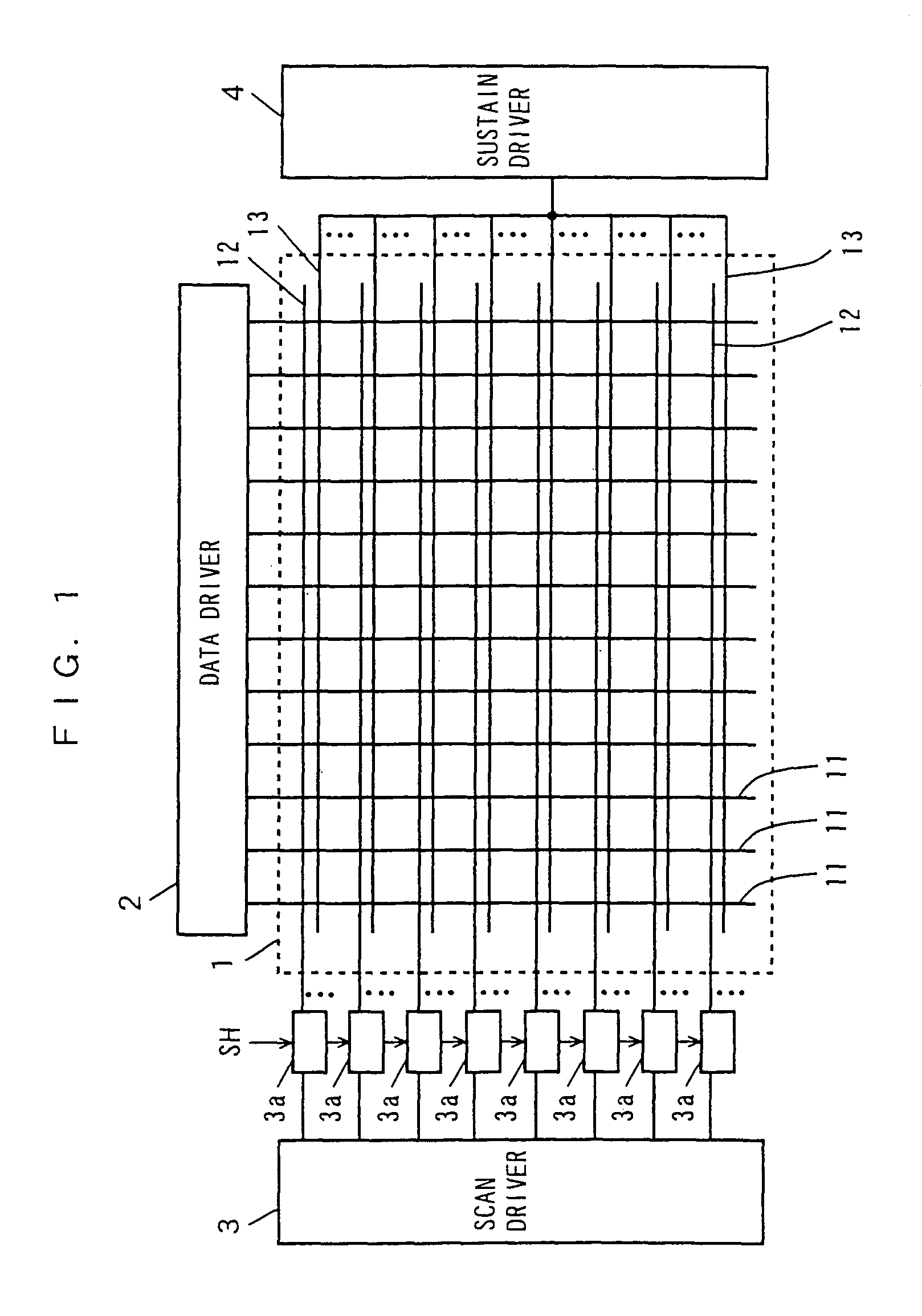
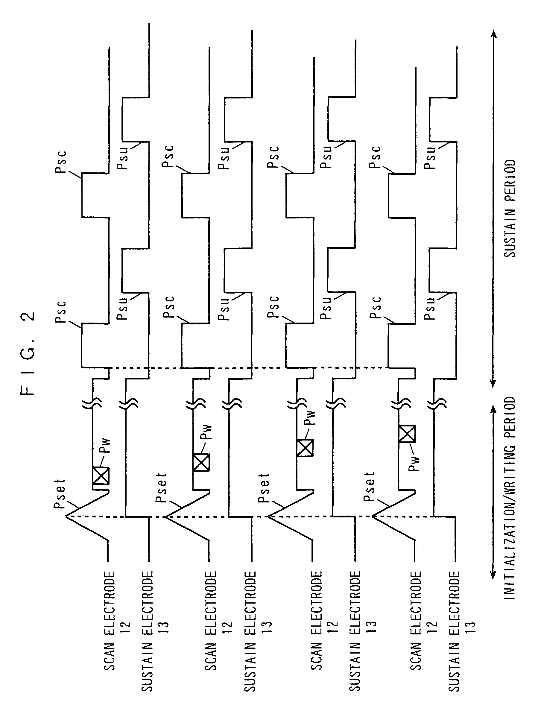
[0069]FIG. 1 is a block diagram showing the configuration of a plasma display device using a sustain driver according to the present invention.
[0070]The plasma display device in FIG. 1 includes a PDP (plasma display panel) 1, a data driver 2, a scan driver 3, a plurality of scan driver ICs (circuits) 3a and a sustain driver 4.
[0071]The PDP 1 includes a plurality of address electrodes (data electrodes) 11, a plurality of scan electrodes 12, and a plurality of sustain electrodes 13. The plurality of address electrodes 11 are arranged in the vertical direction on the screen, while the plurality of scan electrodes 12 and the plurality of sustain electrodes 13 are arranged in the horizontal direction on the screen. The plurality of sustain electrodes 13 are connected together. A discharge cell is formed at each of the intersecting points of the address electrodes 11, the scan electrodes 12 and the sustain electrodes 13 and each discharge cell forms a pixel on the screen.
[0072]The data dr...
second embodiment
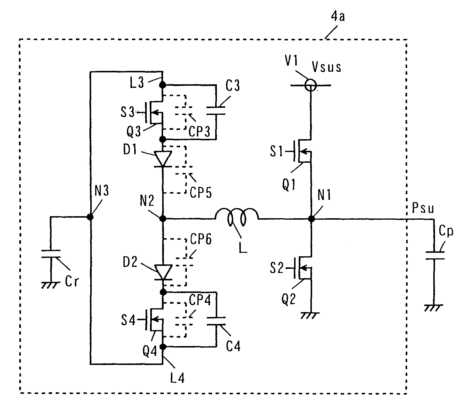
[0105]Other sustain drivers used as the sustain driver 4 in FIG. 1 will be now described. FIG. 6 is a circuit diagram showing the configuration of a sustain driver according to the invention.
[0106]The sustain driver 4a in FIG. 6 is different from the sustain driver 4 in FIG. 3 in that the capacitors C1 and C2 are not provided, and there are additional capacitors C3 and C4 connected in parallel to the transistors Q3 and Q4. The other part is the same as that of the sustain driver 4 shown in FIG. 3, and therefore the same portions are denoted by the same reference characters and are not detailed.
[0107]As shown in FIG. 6, the capacitor C3 is connected in parallel to the drain-source region of the transistor Q3, while the capacitor C4 is connected in parallel to the drain-source region of the transistor Q4. The transistor Q3 has one end connected to the node N3 through the line L3, while the transistor Q4 has one end connected to the node N3 through the line L4. Note that the lines L3 a...
third embodiment
[0122]FIG. 8 is a circuit diagram showing the configuration of a sustain driver according to the present invention.
[0123]The sustain driver 4b in FIG. 8 is different from the sustain driver 4 in FIG. 3 in that the capacitors C1 and C2 are not provided and that there are additional capacitors C5 and C6 connected in parallel to the diodes D1 and D2. The other part is the same as that of the sustain driver 4 in FIG. 3 and therefore the same portions are denoted by the same reference characters and are not detailed.
[0124]As shown in FIG. 8, the capacitor C5 is connected in parallel to the anode-cathode region of the diode D1, and the capacitor C6 is connected in parallel to the anode-cathode region of the diode D2. The cathode of the diode D1 is connected to the node N2 through the line L5, and the anode of the diode D2 is connected to the node N2 through the line L6. The diode D1 has an anode-cathode capacitance CP5 as a parasitic capacitance, and the diode D2 has an anode-cathode capa...
PUM
 Abstract
Description
Claims
Application Information
 - R&D Engineer
- R&D Manager
- IP Professional
- Industry Leading Data Capabilities
- Powerful AI technology
- Patent DNA Extraction
Browse by: Latest US Patents, China's latest patents, Technical Efficacy Thesaurus, Application Domain, Technology Topic.
© 2024 PatSnap. All rights reserved.Legal|Privacy policy|Modern Slavery Act Transparency Statement|Sitemap