Chip testing within a multi-chip semiconductor package

a technology of semiconductor devices and chips, applied in the direction of information storage, static storage, digital storage, etc., can solve the problems of secondary chips that are not able to “talk” or communicate directly through external connectors, and cannot be tested fully

Inactive Publication Date: 2006-11-21
RAMBUS INC
View PDF56 Cites 41 Cited by
  • Summary
  • Abstract
  • Description
  • Claims
  • Application Information

AI Technical Summary

Benefits of technology

[0021]A more complete understanding of the system and method for testing a secondary chip within a multi-chip packaged semiconductor device will be afforded to those skilled in the art, as well as a realization of additional advantages thereof, by a consideration of the following detailed description of one or more embodiments. Reference will be made to the appended sheets of drawings that will first be described briefly.

Problems solved by technology

However, system 100 can be relatively large and may require more space than is available for many types of electronic devices such as cellular telephones, laptops, and personal digital assistants.
Thus, secondary chips generally are not able to “talk” or communicate directly through external connectors.
A drawback of conventional multi-chip packaged semiconductor devices, such as MCM 200, is that it does not allow complete testing of the secondary chips once they are incorporated into the package.
However, even the most rigorous die testing prior to assembly will not guarantee that the assembled MCM will function as desired.
For example, some chips may become damaged during assembly (i.e., after die testing) or the die connections may be faulty within the MCM.
Consequently, a number of MCM failures are the result of integrated circuit chips that have not been fully tested.
Often, these failures are not discovered until after incorporation into an electronic device, which adds to the cumulative cost of the defective MCM, not only for the MCM manufacturer, but also for their customers whose products fail to function properly due to the defective MCM.

Method used


Image

  • Chip testing within a multi-chip semiconductor package
  • Chip testing within a multi-chip semiconductor package
  • Chip testing within a multi-chip semiconductor package

Examples


Embodiment Construction

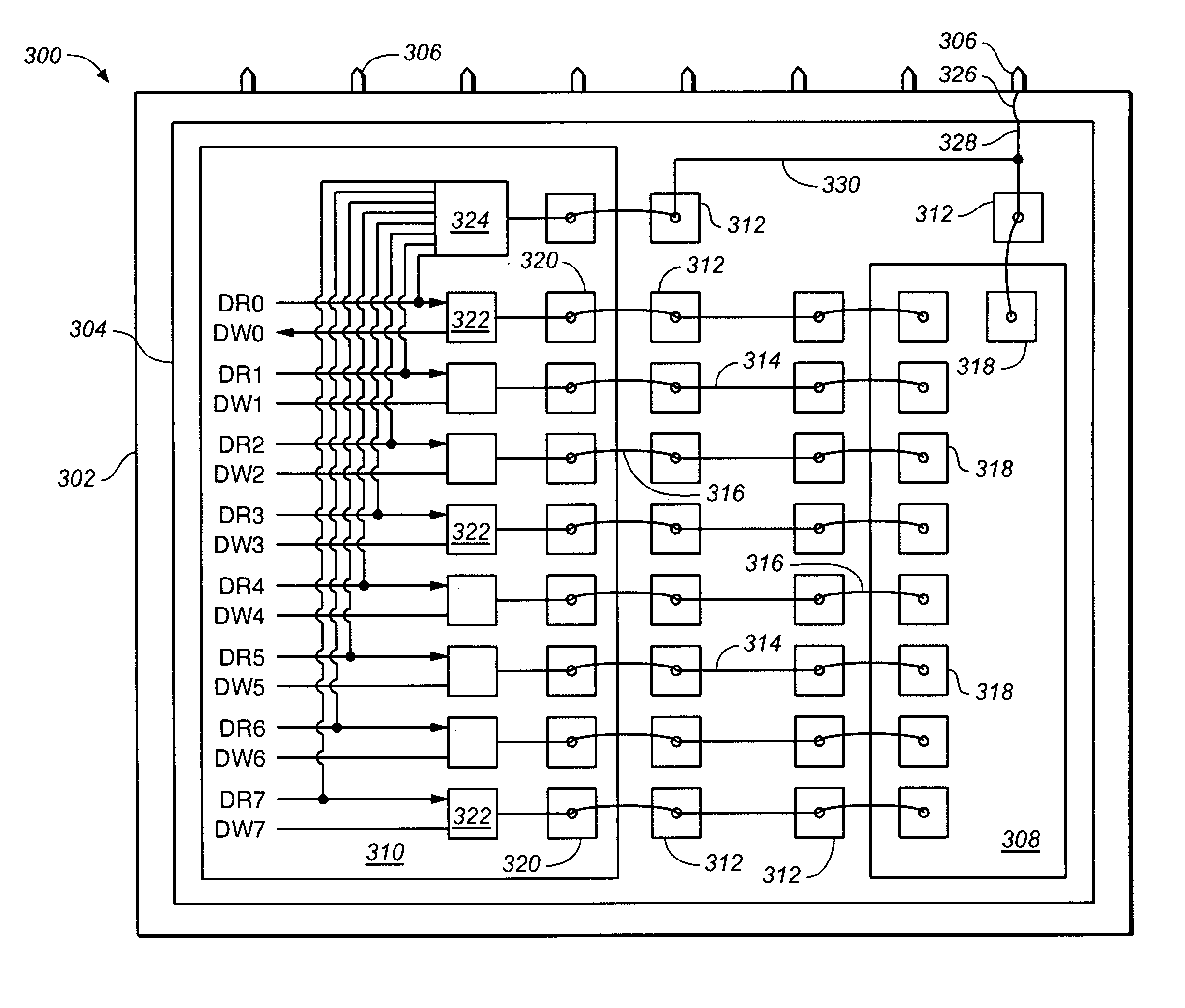
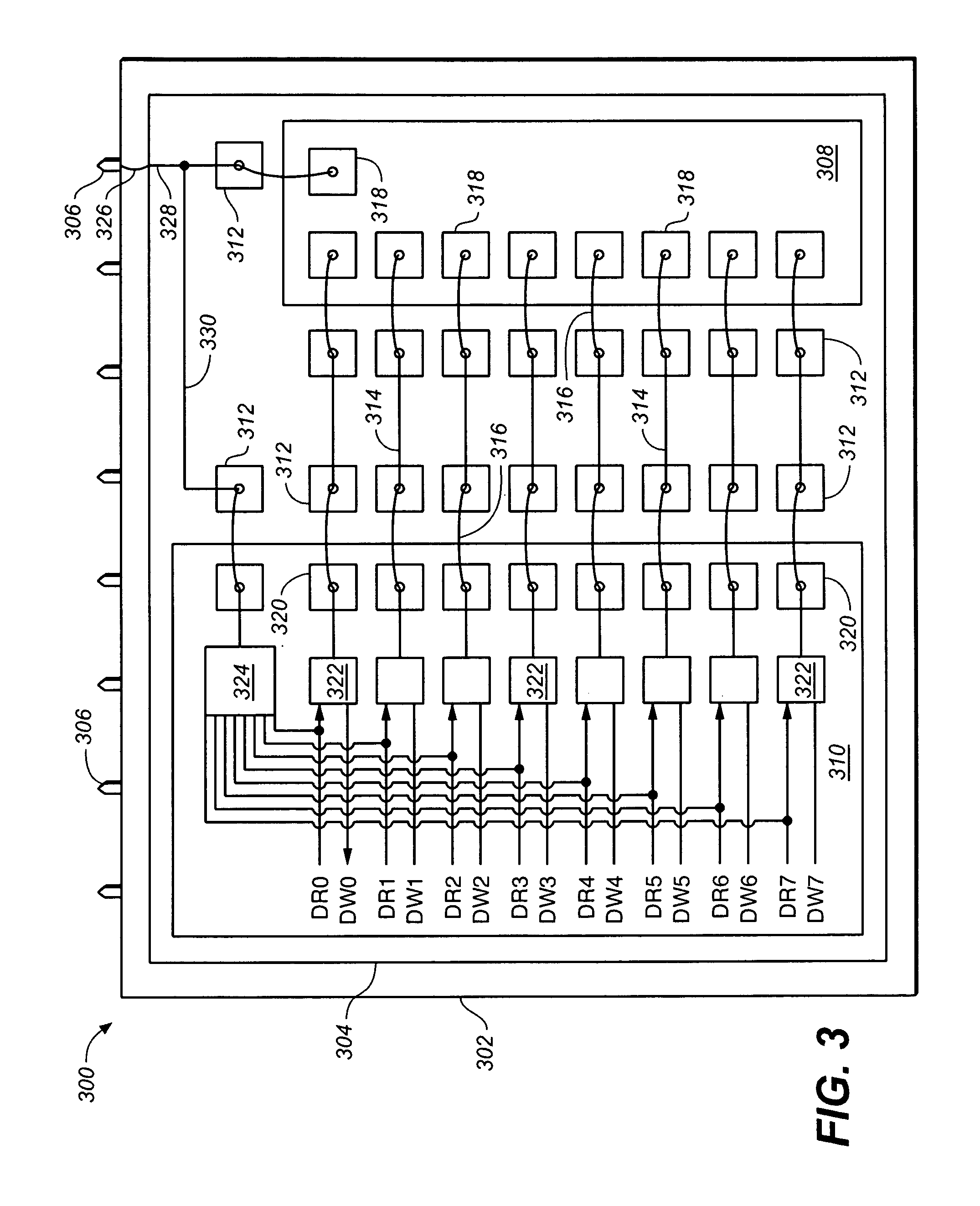
[0033]The present invention provides a system and method for testing one or more secondary chips within a multi-chip packaged semiconductor device. The secondary chip may comprise any type of chip that lacks sufficient connections to external pins or terminals of the multi-chip package to allow complete testing of the secondary chip. For example, a secondary chip may comprise a memory subsystem, a co-processor subsystem, an analog subsystem, or other application-type specific subsystem. A secondary chip comprised of a memory chip is selected as an exemplary application in accordance with an embodiment of the present invention and described in detail below. However, it should be understood that the principles of the present invention are applicable for other types of secondary chips within a semiconductor package and are not limited to exemplary embodiments described herein.

[0034]FIG. 3 is a block diagram illustrating a multi-chip module (MCM) 300 in accordance with an embodiment of ...


PUM


Abstract

A system and method is provided for testing a secondary chip housed within a multi-chip packaged semiconductor device. The packaged semiconductor device includes a secondary chip and a primary chip, with the secondary chip communicating with the primary chip through signal drivers. The secondary chip also includes at least one test signal driver connected to the signal drivers and to certain external connectors that may be shared with the primary chip. The test signal drivers provide testing of the secondary chip using standard integrated circuit test equipment while the secondary chip is contained within the packaged semiconductor device.

Description

CROSS-REFERENCE TO RELATED APPLICATION AND CLAIM OF PRIORITY[0001]The present application is a continuation of U.S. patent application Ser. No. 09 / 666,208, filed on Sep. 21, 2000 now U.S. Pat. No. 6,732,304, entitled “Chip Testing Within A Multi-Chip Semiconductor Package,” which is assigned to the present assignee and hereby incorporated by reference in its entirety.BACKGROUND OF THE INVENTION[0002]1. Field of the Invention[0003]The present invention relates generally to the testing of semiconductor devices and, more particularly, to the testing of chips within a multi-chip packaged semiconductor device.[0004]2. Related Art[0005]Semiconductor devices have continually evolved to provide improvements such as miniaturization, increased speed, reduced power consumption, and reduced cost. As an example, memory is an essential part of an electronic system because it stores information required by the system, such as computational instructions, preliminary calculation data, temporary data...

Claims


Application Information

Patent Timeline
Patent Type & Authority Patents(United States)
IPC IPC(8): G11C29/04G11C29/54G11C29/48
CPCG11C29/1201G11C29/48G11C2207/104
Inventor ONG, ADRIAN E.
Owner RAMBUS INC
Why Eureka
Try Eureka