Semiconductor display device and method of driving a semiconductor display device

a display device and semiconductor technology, applied in the direction of instruments, computing, electric digital data processing, etc., can solve the problems of screen flicker, increased cost, and the drive frequency of the electronic device that generates the image signal cannot handle the image signal frequency, so as to prevent the generation of stripes, the effect of increasing frame frequency and preventing the reduction of the brightness of the overall display screen

Inactive Publication Date: 2006-11-28
SEMICON ENERGY LAB CO LTD
View PDF16 Cites 20 Cited by
  • Summary
  • Abstract
  • Description
  • Claims
  • Application Information

AI Technical Summary

Benefits of technology

[0052]Further, in accordance with using frame inversion in particular with the present invention, the development of stripes due to a phenomenon referred to as disclination between adjacent pixels can be suppressed, and drops in the brightness of the image displayed over an entire screen can be prevented. Disclination is a phenomenon in which an electric field develops between pixel electrodes to which a positive display signal is input, and pixel electrodes to which a negative display signal is input, and the orientation of liquid crystal molecules becomes disordered. The distance between pixel electrodes of adjacent pixels becomes shorter when the pixels are made more high definition, and therefore the electric field between the pixel electrodes becomes larger, and the aperture ratio is seen to drop remarkably due to the disclination. The use of frame inversion in particular by the present invention is therefore effective in that the brightness of the overall display screen is not reduced.
[0056]The frame frequency can therefore be increased without increasing the frequency of the image signal input to an IC, there is no load placed on electronic equipment which generates the image signal, and clear display of a high definition image can be performed with flicker, vertical stripes, horizontal stripes, and diagonal stripes being difficult to see by an observer.
[0057]Further, by using frame inversion in particular with the present invention, the generation of stripes due to the phenomenon referred to as disclination between adjacent pixels can be suppressed, and a reduction in the brightness of the overall display screen can be prevented.
[0058]The time average of the electric potential of the display signals input to each pixel become very close to the opposing electric potential, and this is very effective in preventing degradation of liquid crystals compared to a case of inputting different display signals into each pixel during each frame period.

Problems solved by technology

However, there are times when screen flicker, vertical stripes, horizontal stripes, or diagonal stripes are visible if the above alternating current drive methods are used.
If the frequency of the image signal is raised, it then becomes necessary to increase the specification of electronic devices for generating the image signal, and the cost is increased.
Further, the drive frequency of the electronic devices that generate the image signal becomes unable to handle the image signal frequency, and a load is imparted on the electronic devices that generate the image signals.
Operation may become impossible, and there is the possibility that difficulties will develop due to reliability.

Method used


Image

  • Semiconductor display device and method of driving a semiconductor display device
  • Semiconductor display device and method of driving a semiconductor display device
  • Semiconductor display device and method of driving a semiconductor display device

Examples


embodiment 1

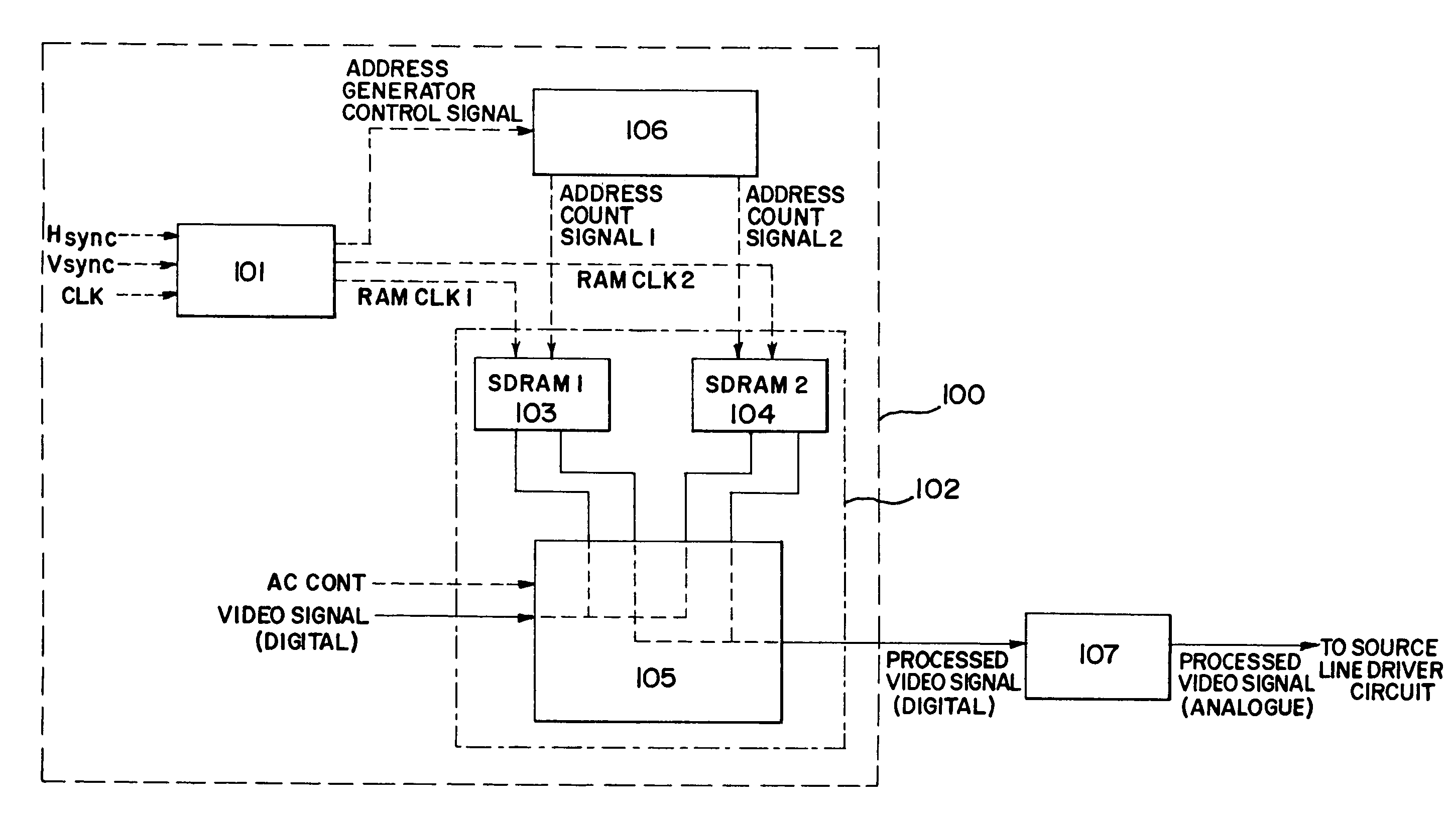
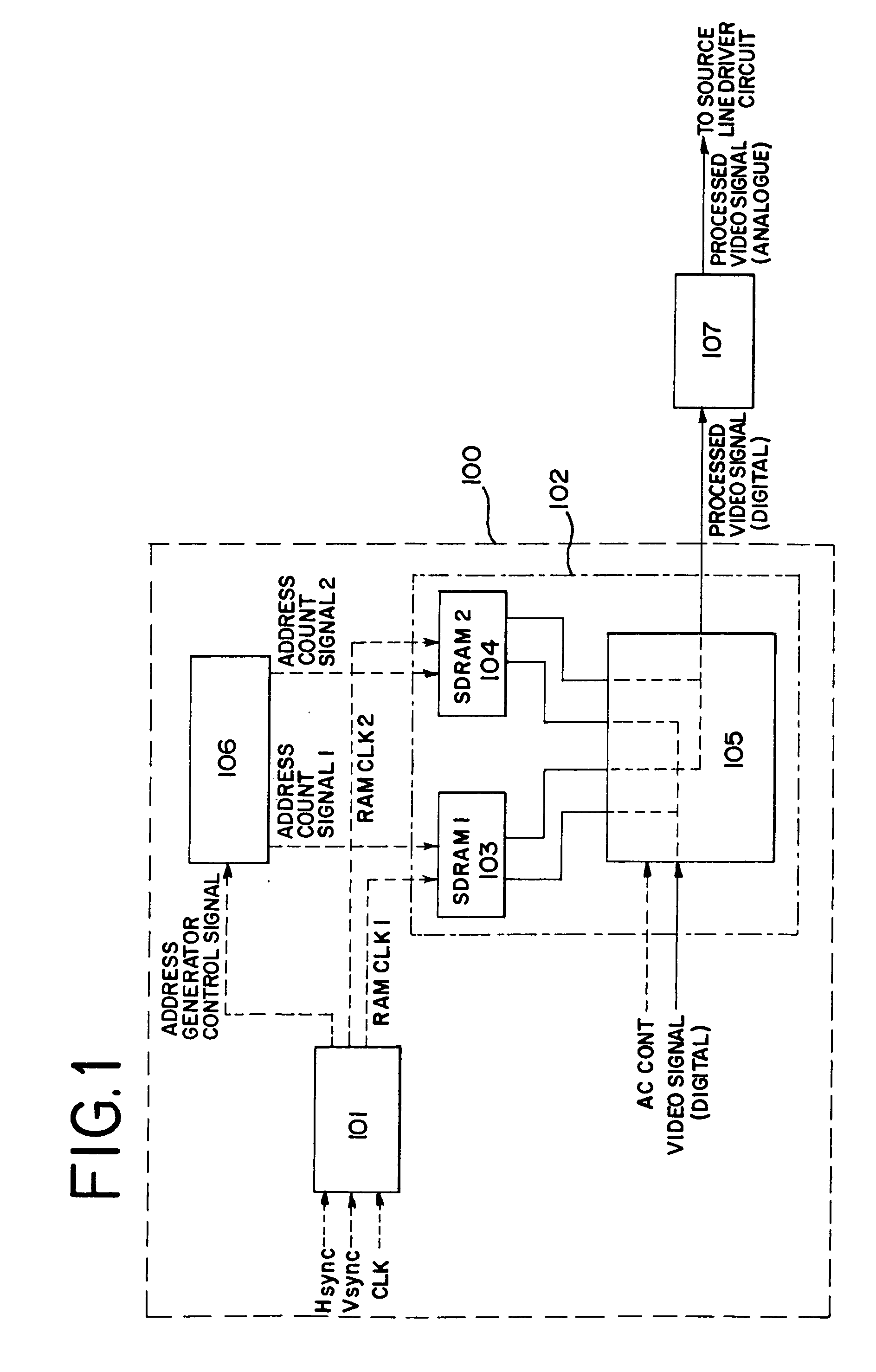
[0305]Input and output timing of an image signal in the first SDRAM 103 and the second SDRAM 104 of FIG. 1 are explained in Embodiment 1 using an example which differs from that of FIG. 3.

[0306]The first and the second read out periods are shorter than the write in period in Embodiment 1. A blank period during which write in and read out of the image signal is not performed is then provided after completion of a first and a second read out periods and before the start of a next write in period.

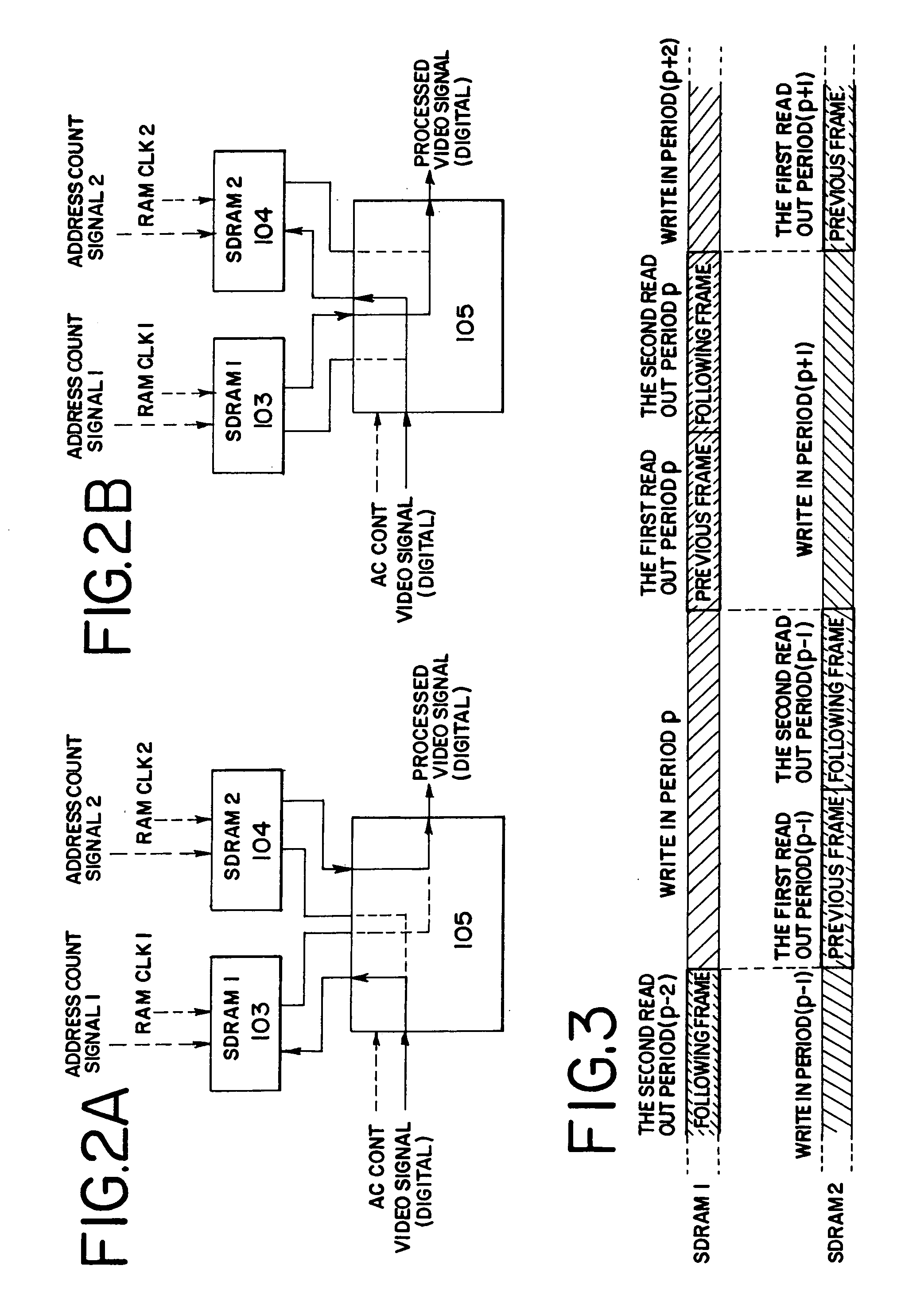
[0307]Image signal write in and read out timing for the first SDRAM 103 and the second SDRAM 104 is shown in FIG. 10. The image signal is written to the first SDRAM 103 in the write in period p. The image signal input to the first SDRAM 103 in a write in period p is then read out two times, in a first read out period p and in a second read out period p.

[0308]Further, the image signal is written to the second SDRAM 104 in a write in period (p−1). The image signal input to the second SDRAM 104 i...

embodiment 2

[0315]Input and output timing of an image signal in the first SDRAM 103 and the second SDRAM 104 of FIG. 1 are explained in Embodiment 2 using an example which differs from that of FIG. 3 and FIG. 10.

[0316]The first and the second read out periods are longer than the write in period in Embodiment 2. A blank period during which write in and read out of the image signal is not performed is then formed after completion of the write in period and before the start of a next is first read out period.

[0317]Image signal write in and read out timing for the first SDRAM 103 and the second SDRAM 104 is shown in FIG. 11. The image signal is written to the first SDRAM 103 in a write in period p. A blank period appears after the write in period p. The blank period is a period during which write in and read out of the image signal is not performed.

[0318]The image signal input to the first SDRAM 103 in the write in period p is then read out two times, in a first read out period p and in a second re...

embodiment 3

[0327]An example of a frame rate conversion portion, differing from that of FIG. 1, of a semiconductor display device of the present invention is explained in Embodiment 3 using FIG. 12.

[0328]The frame rate conversion portion has there SDRAMs in Embodiment 3.

[0329]A frame rate conversion portion 200 has a control portion 201, a frame frequency conversion portion 202, and an address generator portion 206. Further, the frame frequency conversion portion 202 has a first SDRAM (SDRAM 1) 203, a second SDRAM (SDRAM 2) 204, a third SDRAM (SDRAM 3) 207, and a date format portion 205. Reference numeral 208 denotes a D / A converter circuit, which converts an image signal output from the frame rate conversion portion 200 from digital to analog.

[0330]Note that although the frame frequency conversion portion 202 has three SDRAMs (the first SDRAM 203, the second SDRAM 204, and the third SDRAM 207) in Embodiment 3, the number of SDRAMs is not limited to three.

[0331]An Hsync signal, a Vsync signal, ...


PUM


Abstract

A semiconductor display device capable of performing clear display of a high definition image, in which flicker, vertical stripes, horizontal stripes, and diagonal stripes are unlikely to be seen by an observer, is provided. An image signal input from the outside to a RAM of a frame conversion portion in a semiconductor display device is written in, and the written in image signal is read out two times, in order. A period for reading out the image signal input to the RAM one time is shorter than a period for writing in the image signal to the RAM. The electric potentials of display signals input to each pixel in two consecutive frame periods are inverted, with the electric potential of opposing electrodes (opposing electric potential) as a reference, whereby the same image is displayed in a pixel portion in the two consecutive frame periods.

Description

BACKGROUND OF THE INVENTION[0001]1. Field of the Invention[0002]The present invention relates to a suitable method of driving a semiconductor display device using a display medium such as liquid crystals or EL (electro luminescence), and to a semiconductor display device using the driving method. Furthermore, the present invention relates to an electronic device using the semiconductor device display device.[0003]2. Description of the Related Art[0004]Techniques for manufacturing elements formed using semiconductor thin films on an insulating substrate, for example a thin film transistor (TFT), have advanced rapidly in recent years. The reason for these advancements is that the need for semiconductor display devices (typically active matrix liquid crystal display devices) has increased.[0005]An active matrix liquid crystal display device is a device which displays an image by controlling the electric charge applied to between several hundreds of thousands and several millions of pix...

Claims


Application Information

Patent Timeline
Patent Type & Authority Patents(United States)
IPC IPC(8): G09G5/00G09G3/20G09G3/36G09G5/399
CPCG09G3/3614G09G3/20G09G5/399G09G2320/0247G09G3/36
Inventor HIROKI, MASAAKISATO, EIJIONOYA, SHIGERUINOUE, NOBORU
Owner SEMICON ENERGY LAB CO LTD
Why Eureka
Try Eureka