Method and device for masking ringing in a DDR SDRAM

a ddr sdram and masking technology, applied in the field of preventing write failures, can solve the problems of increasing the probability of write failure, not always generated, and causing write failures

Active Publication Date: 2006-11-28
SK HYNIX INC
View PDF7 Cites 23 Cited by
  • Summary
  • Abstract
  • Description
  • Claims
  • Application Information

AI Technical Summary

Benefits of technology

[0021]Accordingly, the present invention has been made to solve the above-mentioned and other problems related to the prior art. An object of the present invention is to provide a method and device for masking ringing in a Double. Data Rate Synchronous Dynamic Random Access Memory (DDR SDRAM) by controlling a DQS buffer to prevent a DQS signal corrupted by a ringing from passing the DQS buffer.
[0036]The means (300, 310, 320, 340, 350) disables the DQS buffer for a mask time (dsb) after accessing all data bursts. The mask time (dsb) is calculated based on at least the second access signal (dsft2) and the data burst length (n). The calculated mask time sufficiently includes the duration of time in which a ringing is present in the DQS signal, so that the disablement of the DQS buffer (330) during the mask time (dsb) prevents a write failure caused by the corrupted DQS signal with the ringing.

Problems solved by technology

In general, a write failure caused by the presence of a ringing in the DQS signal in a write operation is not always generated in all motherboards.
However, the write failure tends to increase as the number of memory module slots on the motherboard increases, as the clock frequency increase, and so forth as the failure may be dependent on various different development techniques utilized in developing a DDR SDRAM.
Therefore, the conventional DDR SDRAM has a problem, in that a conventional DDR SDRAM would regard the ringing present in the DQS signal as a part of the normal DQS signal and thereby would latch the wrong data at the rising and falling edges of the ringing.

Method used


Image

  • Method and device for masking ringing in a DDR SDRAM
  • Method and device for masking ringing in a DDR SDRAM
  • Method and device for masking ringing in a DDR SDRAM

Examples


Embodiment Construction

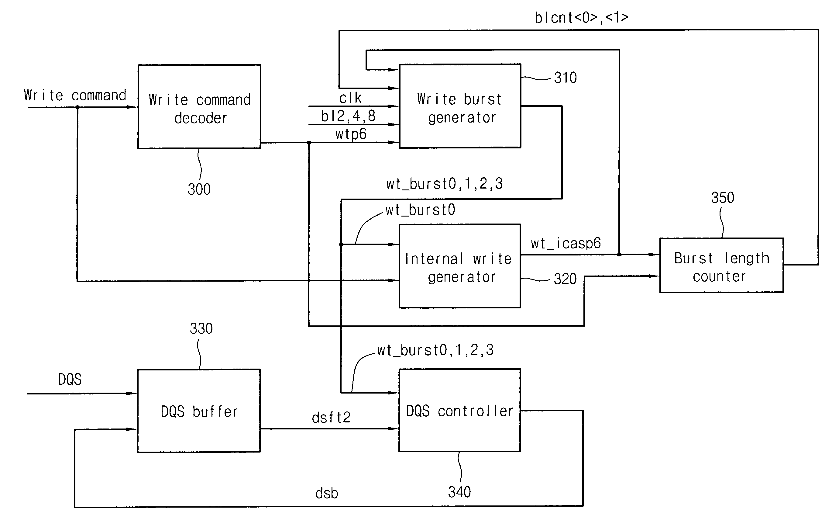
[0051]Hereinafter, the embodiments of the present invention are described with reference to the accompanying drawings. The same reference numerals are used to indicate the same or similar components in the drawings and the description below.

[0052]FIG. 3 is a block diagram showing a device for masking a ringing to prevent write fails in a DDR SDRAM according to an embodiment of the present invention.

[0053]One important operation of the device as shown in FIG. 3 for masking a ringing is to precalculate a point in time at which the ringing is generated when a write command is issued. This point in time at which the ringing is generated is precalculated according to a burst length (e.g., the burst length may be 2, 4, or 8), and this allows a DQS buffer 330 to be disabled before the ringing is generated. For example, the data bust length of 4 is shown in FIG. 4 by the plurality of data 1st_r, 1st_f, 2nd_r, and 2nd_f.

[0054]As shown in FIG. 3, in order to control the DQS buffer 330, the de...


PUM


Abstract

A DDR SDRAM operates at a double data rate by accessing the bursts of data having a burst length in accordance with the rising and falling edges of each pulse of a DQS signal. A ringing may occur in the DQS signal causing write failures. To mask the ringing, a DQS buffer generates a first access signal at the rising edge of each DQS pulse generated in presence of the data burst. The DQS buffer also generates a second access signal at the falling edge of each DQS pulse. Each of the first and second access signals includes a finite number of pulses based on the total number of rising and falling edges of the DQS signal. Two consecutive data bursts are accessed together for a write operation for each pair of the consecutive first and second access signals. After accessing all data bursts, a mask time is calculated to disable the DQS buffer, by which the ringing is masked.

Description

BACKGROUND OF THE INVENTION[0001]1. Field of the Invention[0002]The present invention relates generally to preventing write fails in a memory device including a Double Data Rate Synchronous Dynamic Random Access Memory (DDR SDRAM), and more particularly to preventing write fails that are caused by a ringing in a DQS signal applied to a DDR SDRAM during a write operation.[0003]2. Description of the Prior Art[0004]In general, a Double Data Rate Synchronous Dynamic Random Access Memory (DDR SDRAM) operates at a double speed when compared to the frequency of a clock (clk) signal, because a DDR SDRAM latches or accesses (e.g., reads and writes) data at both the rising and falling edges of a DQS signal during a write operation. In general, the controller of a DDR SDRAM provides the DQS signal (among other signals) during, for example, a write operation, and this DQS signal—at both rising and falling edges—is used to clock data into the DDR SDRAM in a write operation (and into the controll...

Claims


Application Information

Patent Timeline
Patent Type & Authority Patents(United States)
IPC IPC(8): G06F12/00G06F12/16G11C11/40
CPCG11C7/1018G11C7/1078G11C7/1087G11C7/1093G11C11/40
Inventor BAE, SUNG HO
Owner SK HYNIX INC
Why Eureka
Try Eureka