

Wiring design method and system for electronic wiring boards
a wiring design and electronic wiring technology, applied in the field of wiring design system and method, can solve the problems of increasing wiring length or wiring space, and achieve the effect of increasing the accuracy of information and increasing the density of wiring boards
- Summary
- Abstract
- Description
- Claims
- Application Information
AI Technical Summary
Benefits of technology
Problems solved by technology
Method used
Image

Examples
first embodiment
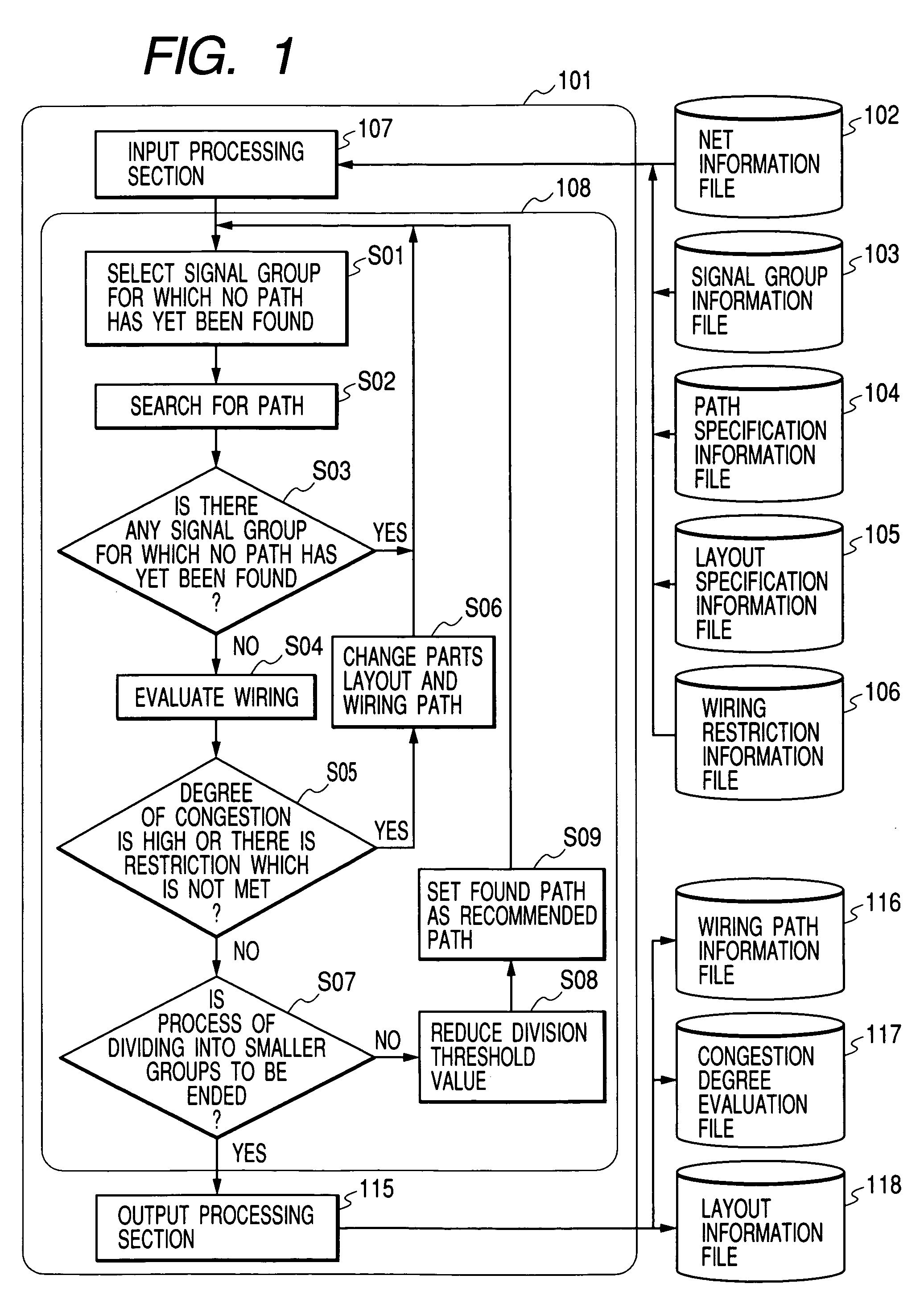
[0090]the present invention will be described below with reference to FIG. 7.
[0091]FIG. 7 is a schematic diagram illustrating processing flow in a wiring design system according to the first embodiment of the present invention.
[0092]The present embodiment generates an optimum wiring design by changing the parts layout and setting a recommended path based on evaluation of the degree of congestion.
[0093]According to the present embodiment, net information 401 on a wiring board 402 indicates that parts 403, 404, 406, 407, 409, and 410 are mounted on the wiring board 402, as shown in the upper-left corner of FIG. 7.
[0094]Connection lines for one signal-group are set between the parts 403 and 404 as connection information 405. Likewise, connection lines for another signal group are set between the parts 406 and 407 as connection information 408. Further, connection lines for still another signal group are set between the parts 409 and 410 as connection information 411.
[0095]The wiring de...
second embodiment
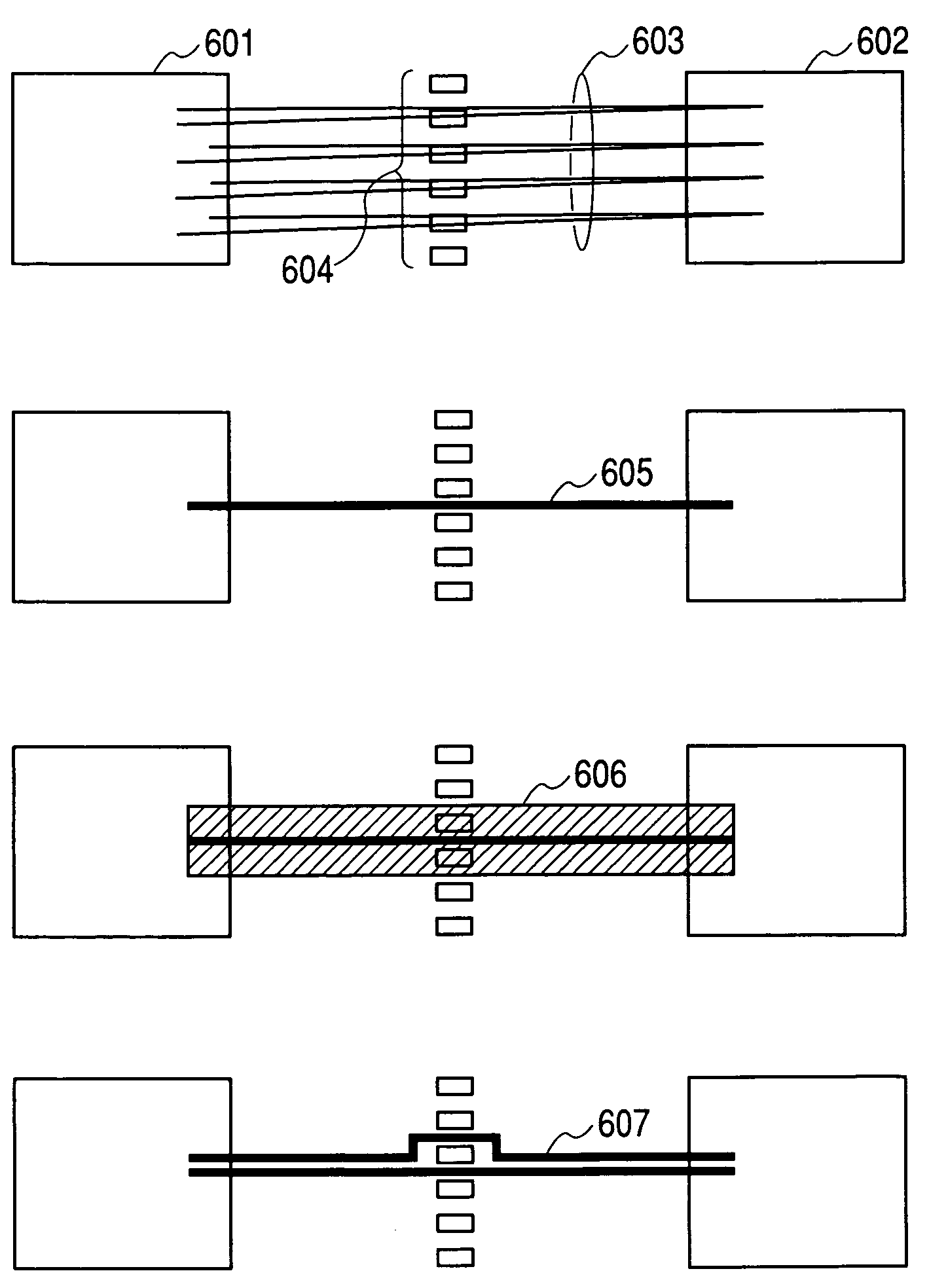
[0101]the present invention will be described below with reference to FIG. 8.
[0102]FIG. 8 is a schematic diagram illustrating processing flow in a wiring design system according to the second embodiment of the present invention.
[0103]The present embodiment designs wiring by considering restrictions on wiring lengths and on distances between neighboring wires.
[0104]Assume, for example, that parts 802 and 803 are mounted on a wiring board 808, and signals 804, 805, 806, and 807 are set between the parts 802 and 803. The signals 804 and 805 belong to one signal group, while the signals 806 and 807 belong to another signal group.
[0105]Furthermore, the wiring board has wiring restrictions. Specifically, a wiring restriction information file 812 contains neighboring wire restriction information 810 and wiring length restriction information 811. The neighboring wire restriction information 810 indicates restrictions on wiring distances between neighboring signal groups, while the wiring le...
third embodiment
[0110]the present invention will be described below with reference to FIG. 9.
[0111]FIG. 9 is a schematic diagram illustrating processing flow in a wiring design system according to the third embodiment of the present invention.
[0112]The present embodiment first generates “temporary wiring” based on temporary information and then changes it into “actual wiring”. The present embodiment is advantageous when it takes a long time to determine a final parts layout, wiring, etc. on a wiring board.
[0113]That is, the wiring design system receives rough information about the wiring board, connections between the parts, and the pin assignments and the layout of parts on the wiring board, and then determines a temporary optimum parts layout and temporary optimum wiring at this point based on the rough information. After that, the wiring design system breaks down the arrangement using detailed information obtained from the temporary optimum parts layout and temporary optimum wiring described abo...
PUM
 Abstract
Description
Claims
Application Information