Semiconductor device and method of manufacturing the same

a semiconductor film and semiconductor technology, applied in the direction of semiconductor devices, electrical equipment, transistors, etc., can solve the problems of forming defects such as grain boundaries, polycrystals, and obtaining polycrystals,

Inactive Publication Date: 2006-12-12
SEMICON ENERGY LAB CO LTD
View PDF46 Cites 55 Cited by
  • Summary
  • Abstract
  • Description
  • Claims
  • Application Information

AI Technical Summary

Benefits of technology

[0013]The present invention has been made in view of the above problems, and an object of the present invention is therefore to provide a semiconductor device composed of a semiconductor element or a group of semiconductor elements, in which a crystalline semiconductor film having as few grain boundaries as possible in a channel formation region is formed on an insulating surface, which can operate at high speed, which have high current drive performance, and which are less fluctuated between elements.
[0019]The semiconductor film is irradiated with laser light or intense light collected into a linear shape and expanded in the longitudinal direction. Moving the laser light irradiation position and the substrate on which the crystalline semiconductor film is formed relatively, laser light runs over a part or the entire surface of the crystalline semiconductor film to melt and crystallize or re-crystallize the crystalline semiconductor film. The laser light scanning direction is set to the longitudinal direction of the opening or the channel length direction of the transistor. This way crystals grow along the laser light scanning direction and grain boundaries or sub-grain boundaries are prevented from crossing the channel length direction.
[0023]By setting the depth of the opening equal to the thickness of the semiconductor film, the semiconductor melted by irradiation of laser light or intense light aggregates and solidifies in the opening (concave) through surface tension. As a result, the semiconductor film is thinned in the opening (convex) to cause the stress deformation to concentrate on the thinned region. The side faces of the opening have an effect of determining the crystal orientation to a certain degree. The angle of the side faces of the opening with respect to the substrate surface is 5 to 90°, preferably 30 to 90°. Laser light runs over the semiconductor film in the direction parallel to the channel length direction, thereby orienting crystals primarily in a specific crystal orientation along the opening extending in this direction.
[0026]The present invention described above makes it possible to specify the location for forming a semiconductor element such as a transistor, in particular, a channel formation region of a TFT, so that a crystalline semiconductor film having no grain boundaries is obtained. This eliminates causes of fluctuation such as randomly-formed grain boundaries and crystal defects, and provides a TFT or a group of TFTs less fluctuated in characteristic.

Problems solved by technology

It is considered that the problem is that the method utilizes level differences of a base as in the known graphoepitaxy technique and crystals grow along the level differences to leave level differences on the surface of the obtained single crystal semiconductor film.
In addition, a single crystal semiconductor film cannot be formed by graphoepitaxy on a glass substrate which has a relatively low distortion point.
On the other hand, when an amorphous semiconductor film formed on a flat surface is crystallized by laser light irradiation, polycrystals are obtained and defects such as grain boundaries are formed at random.
Therefore crystals having the same orientation cannot be obtained.
A grain boundary has a large number of crystal defects, which serve as carrier traps and are considered as the cause of lowering in mobility of electrons or holes.
It has been impossible to form a semiconductor film that has no defects, grain boundaries, or sub-grain boundaries caused by volume shrinkage of a semiconductor, thermal stress with a base, and lattice mismatch which accompany crystallization.
Accordingly, it has been impossible for a crystalline semiconductor film formed on an insulating surface by crystallization or re-crystallization to achieve the quality of a MOS transistor formed on a single crystal substrate without bonding SOI (Silicon on Insulator).
For instance, when a semiconductor film is formed on a glass substrate to build a TFT, the TFT is arranged giving no regard to randomly-formed grain boundaries and therefore the crystallinity of a channel formation region of the TFT cannot be controlled strictly.
The randomly-formed grain boundaries and crystal defects lower the characteristics and cause fluctuation in characteristic between elements.

Method used


Image

  • Semiconductor device and method of manufacturing the same
  • Semiconductor device and method of manufacturing the same
  • Semiconductor device and method of manufacturing the same

Examples


embodiment 1

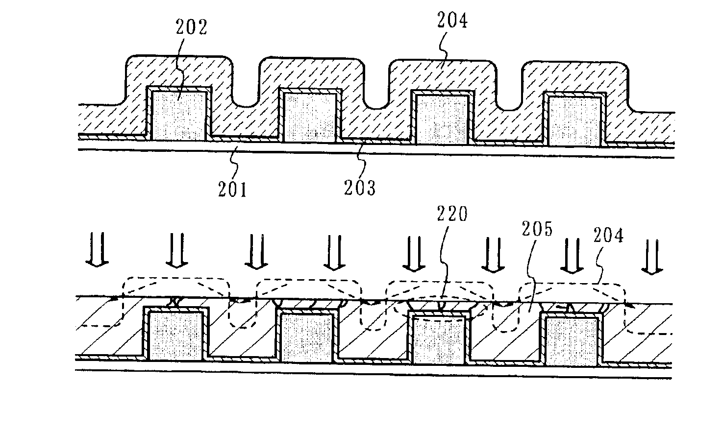
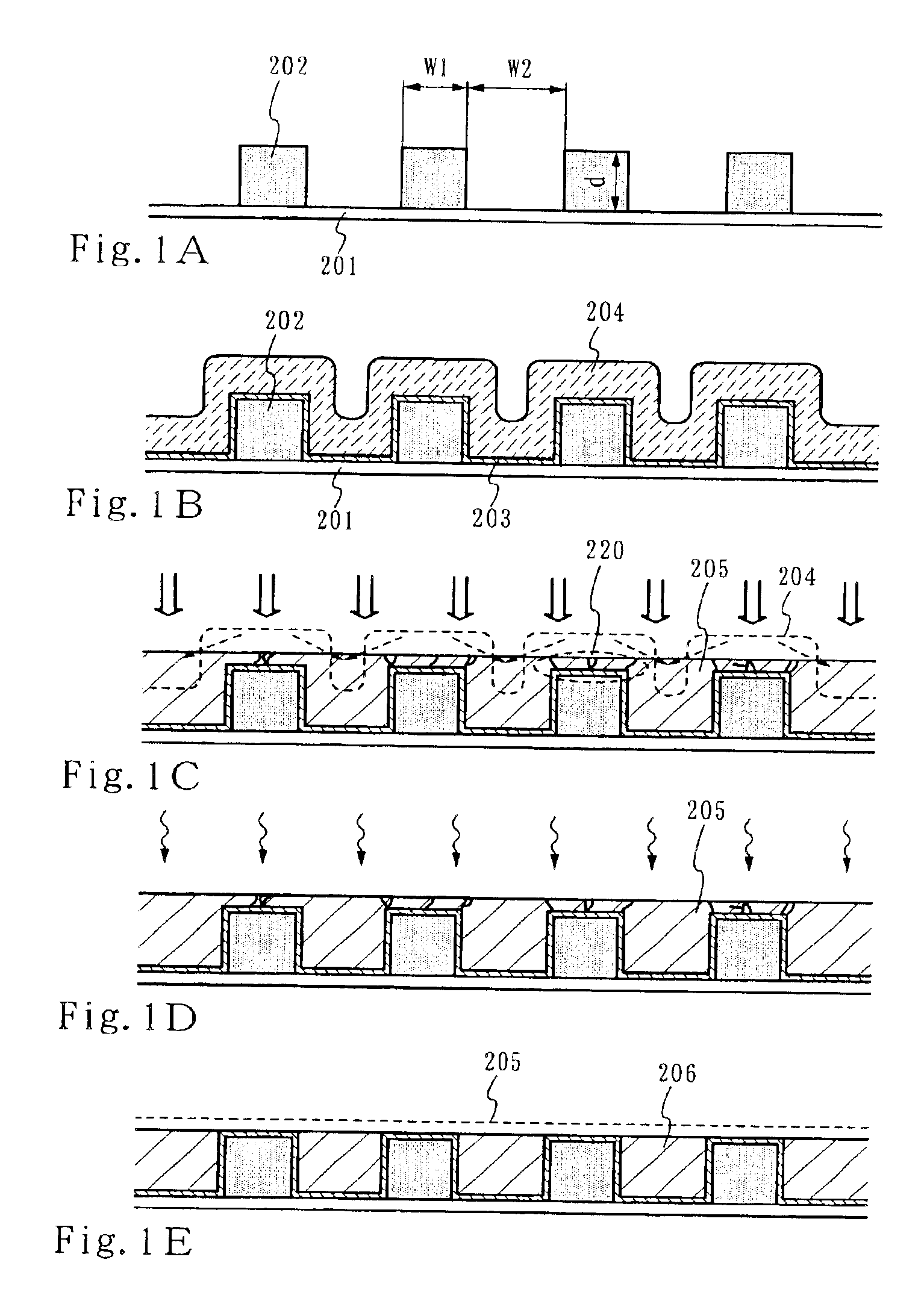
[0097]Referring to FIGS. 1A to 1E, explanations will be given on the above-described mode of the present invention. FIGS. 1A to 1E are vertical sectional views illustrating a process of forming a crystalline semiconductor film of the present invention.

[0098]In FIG. 1A, a first insulating film 201 is formed to a thickness of 30 to 300 nm from silicon nitride, silicon oxynitride whose nitrogen content is larger than its oxygen content, aluminum nitride, or aluminum oxynitride. On the first insulating film 201, a second insulating film 202 is formed from silicon oxide or silicon oxynitride to a thickness of 10 to 1000 nm , preferably 50 to 200 nm . The second insulating film 202 has openings having a desired shape. A desired shape may be a rectangle, a circle, a polygon, a belt, or a shape matching the shape of an island-like semiconductor film (active layer) of a TFT to be manufactured. A silicon oxide film can be formed by plasma CVD using a mixture of tetraethyl ortho silicate (TEOS...

embodiment 2

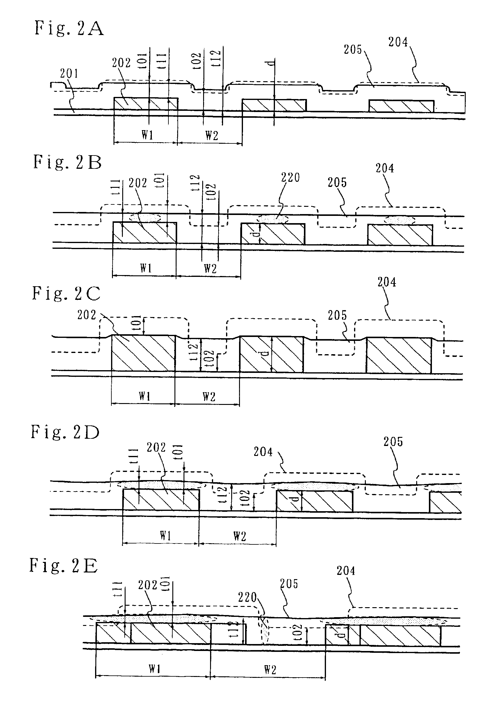
[0116]In forming a crystalline semiconductor film of the present invention, an amorphous semiconductor film crystallized by laser light irradiation as shown in Embodiment 1 may be further irradiated with laser light to melt the film again for re-crystallization.

[0117]FIGS. 3A to 3E show an example thereof. First, a first insulating film 201, a second insulating film 202, a silicon oxynitride film 203, and an amorphous semiconductor film 204 are formed in the manner described in Embodiment 1. The amorphous semiconductor film 204 is doped with Ni as a metal element having catalytic functions for accelerating crystallization, such as lowering the crystallization temperature of silicon and improving the orientation. How the film is doped with Ni is not limited and spin coating, evaporation, sputtering, or other methods can be employed. When spin coating is used, an aqueous solution containing 5 to 10 ppm of nickel acetate is applied to form a metal element-containing layer 210. The cata...

embodiment 3

[0122]This embodiment gives a description with reference to FIGS. 4A to 10F on a mode of manufacturing a TFT whose channel formation region is placed in a filling region. The filling region is a region of a crystalline silicon film that fills an opening of a base insulating film that is formed under the crystalline silicon film. FIG. 4A is a top view whereas FIGS. 4B and the subsequent drawings are vertical sectional views of various portions of FIG. 4A.

[0123]Similarly, FIGS. 5A, 6A, 7A, 8A, 9A, and 10A are top views whereas the rest are vertical sectional views.

[0124]In FIGS. 4A to 4E, a silicon nitride film or aluminum oxynitride film with a thickness of 30 to 300 nm is formed as a first insulating film 302 on a glass substrate 301. On the first insulating film 302, a silicon oxide film or a silicon oxynitride film is formed and subjected to photo etching to form a second insulating film 303 that has rectangular patterns. A silicon oxide film with a thickness of 1000 nm is formed ...


PUM


Abstract

To provide a semiconductor device composed of a semiconductor element or a group of semiconductor elements, in which a crystalline semiconductor film having as few grain boundaries as possible in a channel formation region is formed on an insulating surface, which can operate at high speed, which have high current drive performance, and which are less fluctuated between elements. The method of the present invention includes: forming an insulating film with an opening on a substrate having an insulating surface; forming on the insulating film and over the opening an amorphous semiconductor film or a polycrystalline semiconductor film that has randomly-formed grain boundaries; forming a crystalline semiconductor film by melting the semiconductor film, pouring the melted semiconductor into the opening of the insulating film, and crystallizing or re-crystallizing the semiconductor film; and removing the crystalline semiconductor film except a portion of the crystalline semiconductor film that is in the opening to form a gate insulating film, which is in contact with the top face of the crystalline semiconductor film, and a gate electrode.

Description

BACKGROUND OF THE INVENTION[0001]1. Field of the Invention[0002]The present invention relates to a semiconductor device formed from a semiconductor film that has a crystal structure as well as a method of manufacturing the same, and more specifically, to a semiconductor device including a field effect transistor whose channel formation region is formed from a crystalline semiconductor film on an insulating surface and a method of manufacturing the semiconductor device.[0003]2. Description of the Related Art[0004]A technique of forming an amorphous semiconductor film on a glass or other insulating substrate and crystallizing the film by laser light irradiation is known. A thin film transistor (hereinafter referred to as TFT) manufactured from a semiconductor film having a crystal structure (crystalline semiconductor film) is applied to planar display devices (flat panel displays), typically, liquid crystal display devices.[0005]Laser light is applied to a semiconductor manufacturing ...

Claims


Application Information

Patent Timeline
Patent Type & Authority Patents(United States)
IPC IPC(8): H01L21/84H01L21/336H01L21/77H01L27/12H01L27/32H01L29/04H01L29/786
CPCH01L27/12H01L29/04H01L27/1281H01L29/78675H01L29/78696H01L29/66757H01L27/3244H01L29/78621H10K59/12H01L29/786
Inventor ISOBE, ATSUOYAMAZAKI, SHUNPEIKOKUBO, CHIHOTANAKA, KOICHIROSHIMOMURA, AKIHISAARAO, TATSUYAMIYAIRI, HIDEKAZU
Owner SEMICON ENERGY LAB CO LTD
Why Eureka
Try Eureka