

Page buffer circuit of flash memory device with reduced consumption power
a flash memory device and page buffer technology, applied in static storage, digital storage, instruments, etc., can solve the problem of increasing the consumption power of the page buffer
- Summary
- Abstract
- Description
- Claims
- Application Information
AI Technical Summary
Problems solved by technology
Method used
Image

Examples
Embodiment Construction
[0020]Various embodiments will be described below in more detail with reference to the accompanying drawings. The present invention may, however, be embodied in different forms and should not be constructed as limited to the embodiments set forth herein. Rather, these embodiments are provided so that this disclosure will be thorough and complete. Like numerals refer to like elements throughout the specification.
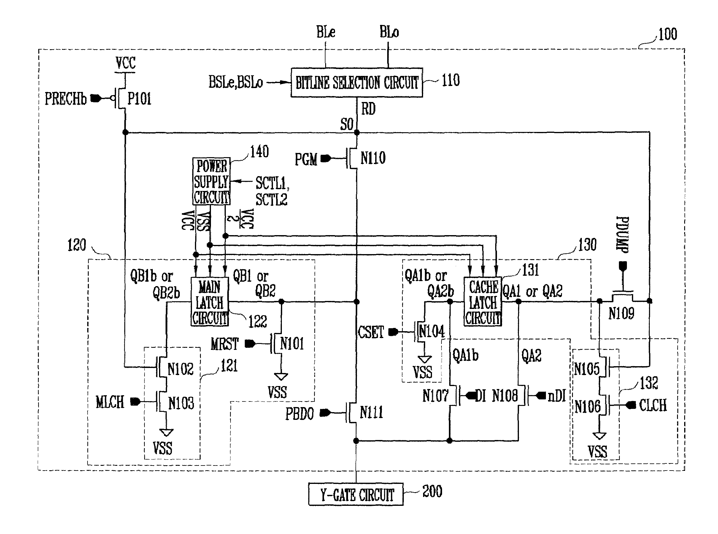
[0021]FIG. 3 is a diagram illustrating a page buffer circuit of a flash memory device.
[0022]Referring to FIG. 3, the page buffer circuit 100 may include a bitline selection circuit 110, a main register circuit 120, a cache register circuit 130, a power supply circuit 140, a precharging circuit P101, and switches N107˜N111. Here, the precharging circuit P101 may be implemented by a PMOS transistor, and the switches N107˜N111 may be constructed of NMOS transistors. Hereinafter, the precharging circuit P101 will be referred to as the PMOS transistor and the switches N107˜N111 wi...
PUM
 Abstract
Description
Claims
Application Information