
Executing debug instructions

a debugging instruction and instruction technology, applied in the field of data processing systems, can solve the problems of requiring switching between clock speeds, reducing the value of diagnostic operations, and not being able to execute instructions at their normal speed,

Inactive Publication Date: 2001-11-20
ARM LTD
View PDF6 Cites 99 Cited by
  • Summary
  • Abstract
  • Description
  • Claims
  • Application Information

AI Technical Summary

Benefits of technology

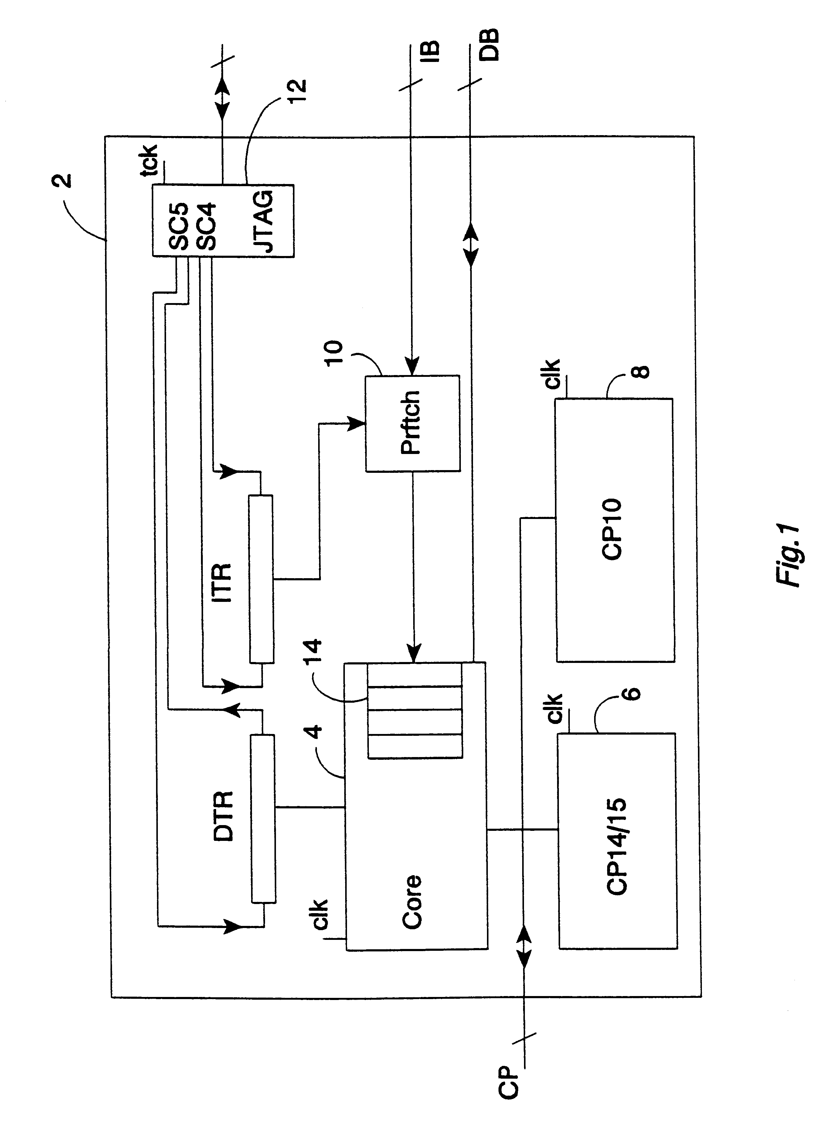
The present invention recognises that the main processor can be left operating at its normal clock speed whilst instructions are loaded by arranging for the main processor to execute no-operations instructions pending the execution of the loaded instruction. When the loaded instruction is present within the instruction transfer register, it can then be issued to the main processor and executed at the normal clock speed without requiring clock switches or resynchronisation.
A preferred mechanism for loading the instruction transfers register is via a serial scan chain. The way in which the main processor continues to operate at its normal clock speed executing no-operation instructions makes the provision of the serial scan chain mechanism simpler as it need not cater to the main processor.
This data transfer register may conveniently be accessed via a serial scan chain and may be split into the form of two data transfer registers to provide bidirectional communications whilst avoiding potential data conflicts.

Problems solved by technology

Whilst the different clock speed facilitates the loading of the instructions into the system (for example via a serial scan chain), it has the disadvantage that the instruction is not executed at its normal speed and so the value of the diagnostic operation is reduced.
Whilst this improves the accuracy and usefulness of the diagnostic operation, it has the disadvantage of requiring switching between clock speeds, clock synchronisation and their associated circuits.

Method used


Image

  • Executing debug instructions
  • Executing debug instructions
  • Executing debug instructions

Examples


Embodiment Construction

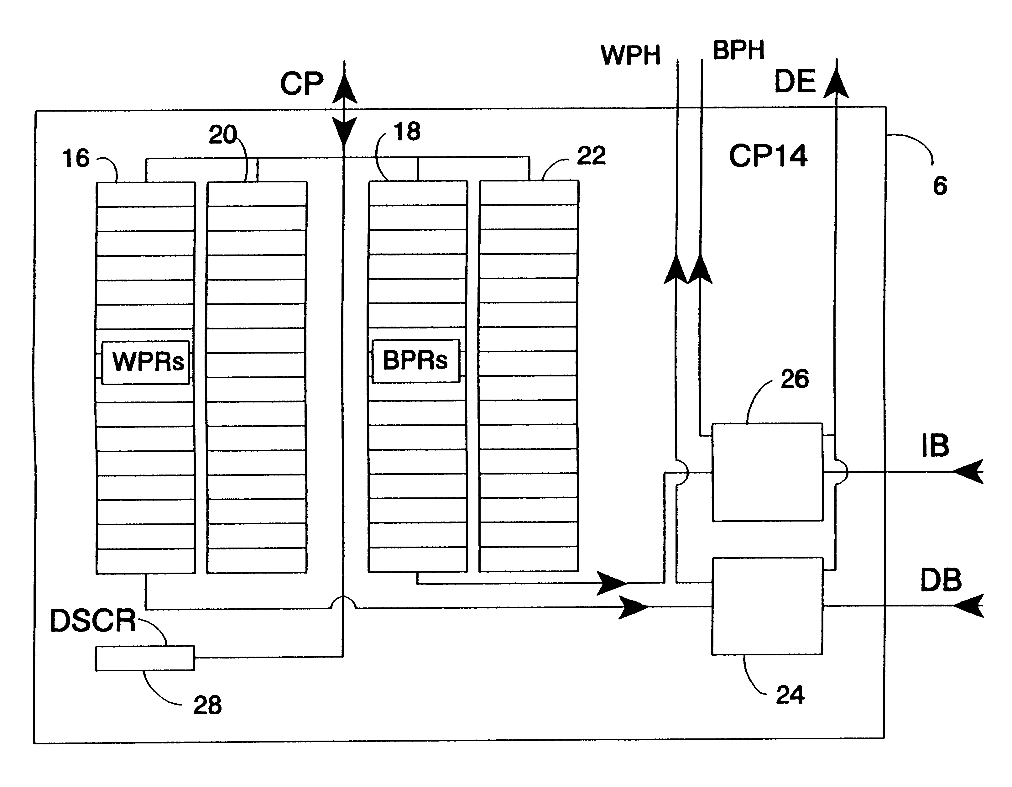
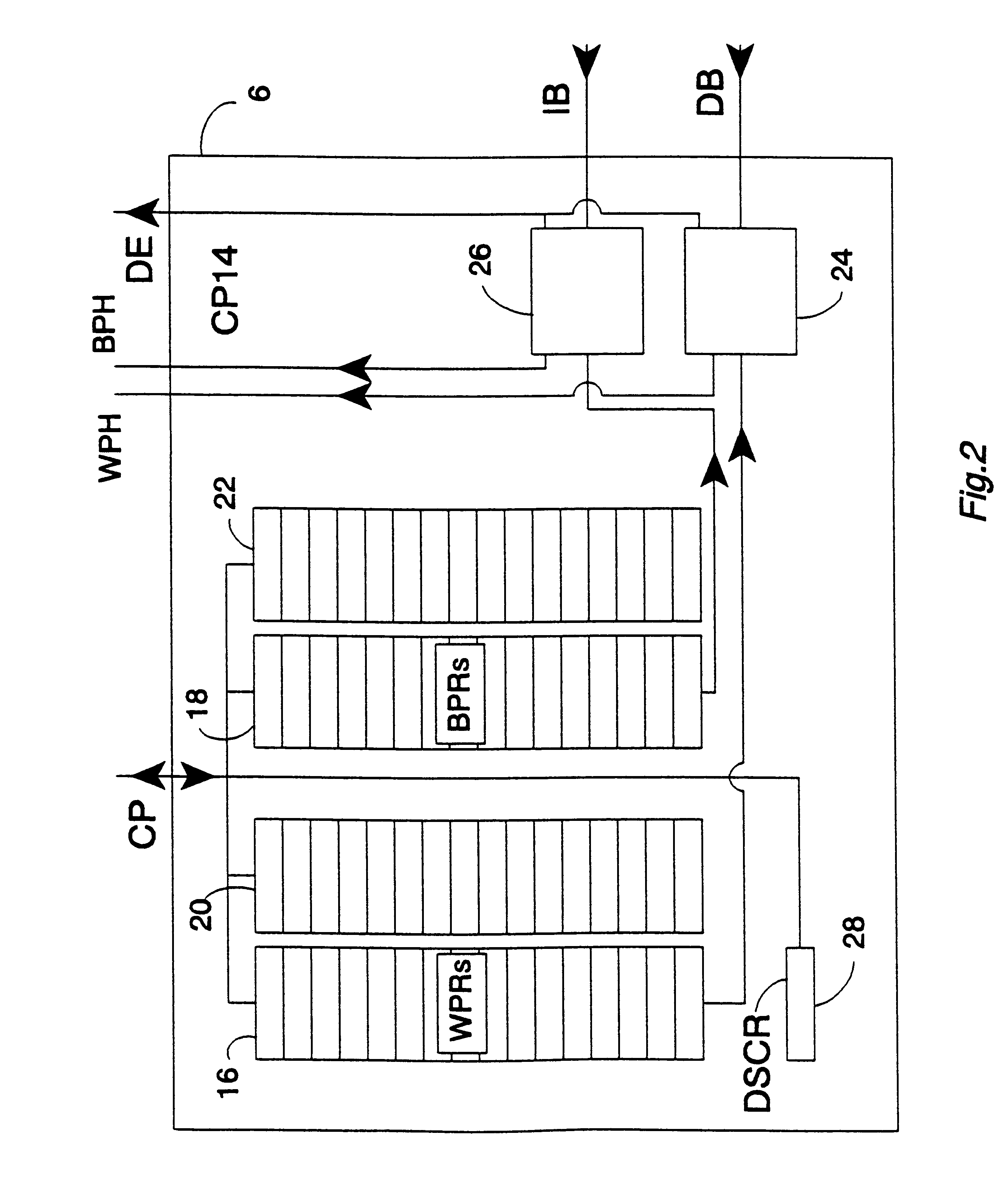
FIG. 1 shows a data processing system 2 that includes a main processor 4, a debug coprocessor (and system coprocessor) 6 and a floating point unit coprocessor 8. The main processor 4 is coupled via a coprocessor interface in the form of a coprocessor bus CP to the debug coprocessor 6 and the floating point unit coprocessor 8. The form of this coprocessor bus CP is substantially the same as a standard coprocessor bus, such as the ARM coprocessor bus (as used with microprocessors produced by ARM Limited of Cambridge, England).

The main processor 4 is coupled to a data bus DB and via a prefetch unit 10 to an instruction bus IB. The data bus DB and the instruction bus IB both include address portions that are monitored by the debug coprocessor 6 to identify breakpoints and watchpoints respectively.

The main processor 4, the debug coprocessor 6 and the floating point unit coprocessor 8 are all driven by a common main processor clock signal clk at a main processor clock frequency. A scan ch...


PUM


Abstract

Apparatus for processing data is provided, said apparatus comprising: a main processor 4 driven by a main processor clock signal clk at a main processor clock frequency; debug logic 6, 12 at least a portion 12 of which is driven by a debug clock signal tck at a debug clock frequency, said debug clock frequency being different to said main processor clock frequency and said main processor clock signal clk being asynchronous with said debug clock signal tck; and an instruction transfer register ITR into which a data processing instruction may be transferred by said debug logic 12 and from which said data processing instruction may be read by said main processor 4; wherein when switched from a normal mode to a debug mode said main processor 4 continues to be driven by said main processor clock signal clk executing no-operation instructions until a data processing instruction is present within said instruction transfer register ITR and said debug logic 12 triggers said main processor to read and execute said data processing instruction whilst still driven by said main processor clock signal clk. This arrangement allows debug instructions to be executed at full speed whilst avoiding the need to switch clock speeds and provide a synchronisation mechanism.

Description

1. Field of the InventionThis invention relates to data processing systems. More particularly, this invention relates to data processing systems incorporating debug mechanisms and the manner in which such systems execute debug instructions.2. Description of the Prior ArtIn order to facilitate the development of new data processing hardware and software it is known to provide dedicated debug mechanisms. Such mechanisms typically allow diagnostic data to be recovered and debug instructions to be executed, such as instructions to recover certain data values to locations from which they can be accessed as diagnostic data. In addition, it may be desired to execute particular instructions that use particular features or portions of the system being debugged to test the operation of those particular features or portions.Some known data processing systems operate in the debug mode by switching to a different clock speed (typically slower) than the normal operation clock speed and then loadi...

Claims


Application Information

Patent Timeline
Patent Type & Authority Patents(United States)
IPC IPC(8): G06F11/36G06F11/22G06F11/28G06F9/38
CPCG06F11/3632G06F11/3648
Inventor JAGGAR, DAVID VIVIANHOHL, WILLIAM ADAM
Owner ARM LTD
Learn More