

Cascaded delay locked loop circuit
a delay lock and loop technology, applied in the direction of angle demodulation by phase difference detection, automatic control of pulses, electrical apparatus, etc., can solve the problem that the frequency resolution obtainable with known technology is inadequate when considered
- Summary
- Abstract
- Description
- Claims
- Application Information
AI Technical Summary
Benefits of technology
Problems solved by technology
Method used
Image

Examples
Embodiment Construction
[0018]While this invention is susceptible of embodiment in many different forms, there is shown in the drawings and will herein be described in detail specific embodiments, with the understanding that the present disclosure is to be considered as an example of the principles of the invention and not intended to limit the invention to the specific embodiments shown and described. In the description below, like reference numerals are used to describe the same, similar or corresponding parts in the several views of the drawings.
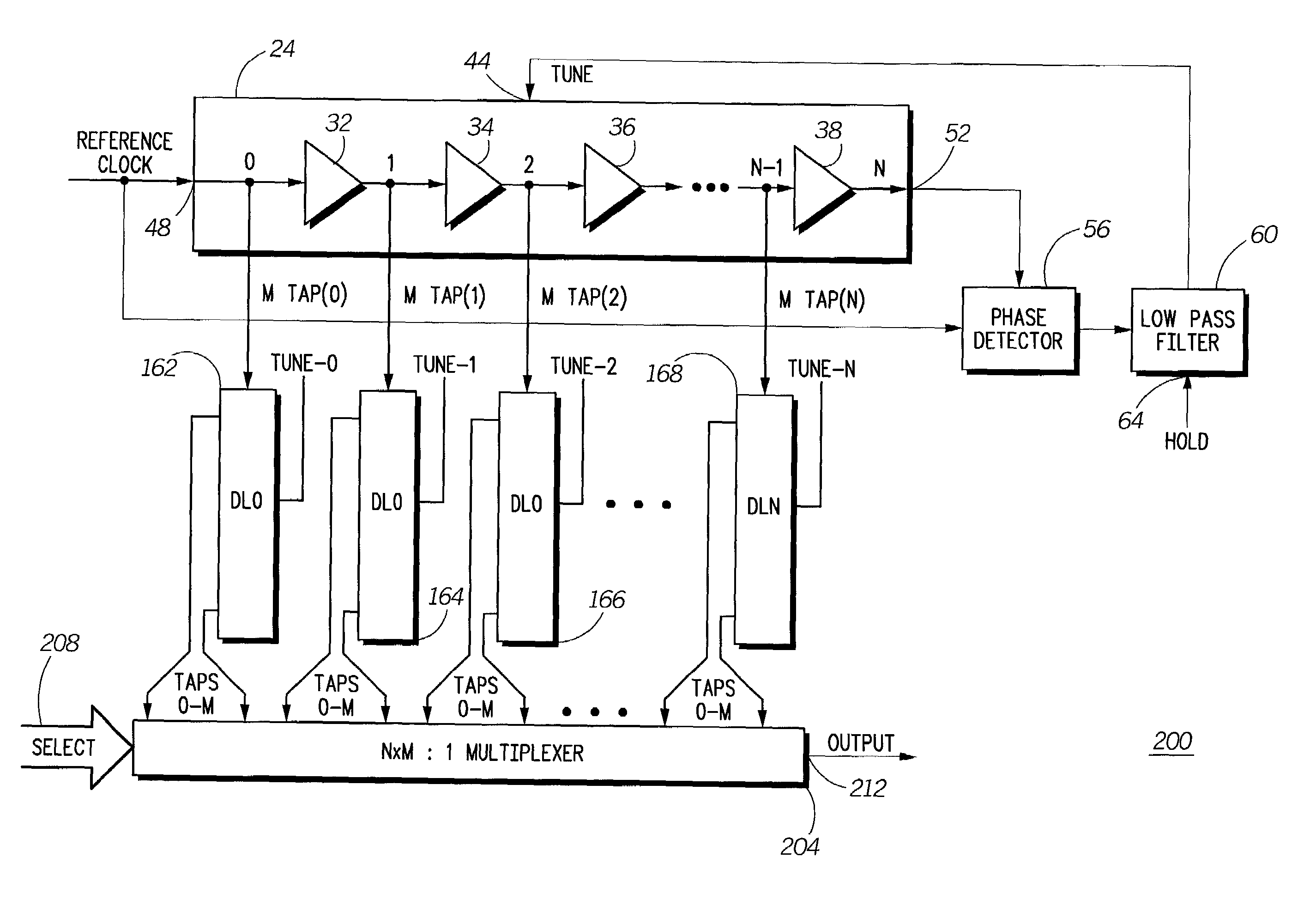
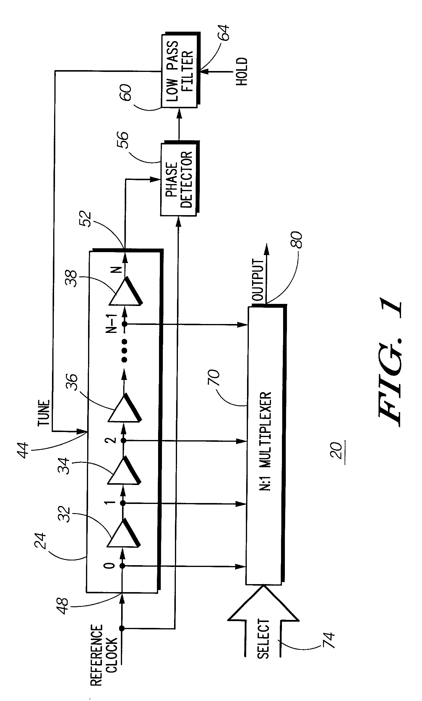
[0019]Turning now to FIG. 1, a basic delay locked loop circuit 20 is illustrated. This circuit is similar to that found in U.S. patent application Ser. No. 09 / 633,705 filed Aug. 7, 2000 to Frederick Lee Martin entitled “Digital-To-Phase Converter” which is hereby incorporated by reference. In this delay locked loop circuit 20, a delay line 24 is made up of a plurality of cascaded controlled delay elements 32, 34, 36 through 38, each having an input and an output...
PUM
 Abstract
Description
Claims
Application Information