Ozone vapor clean method

a technology of ozone vapor and cleaning method, which is applied in the direction of semiconductor/solid-state device manufacturing, basic electric elements, electric apparatus, etc., can solve the problems of non-uniform thickness of pre-liner oxide films, adverse effects on device performance and reliability, and compromise of device functional integrity in finished electronic products

Inactive Publication Date: 2007-01-02
TAIWAN SEMICON MFG CO LTD
View PDF2 Cites 147 Cited by
  • Summary
  • Abstract
  • Description
  • Claims
  • Application Information

AI Technical Summary

Problems solved by technology

Accordingly, device performance and reliability can be adversely affected by such factors as interfacial defects, defect precursors and diffusion of dopants through gate dielectrics, as well as unintended variations in thickness in the gate oxide layer among central and peripheral regions of the layer.
Moreover, the presence of particles in the integrated circuits compromises the functional integrity of the devices in the finished electronic product.
However, this mode of bringing oxygen into contact with the wafer surface has resulted in the formation of pre-liner oxide films of non-uniform thickness.
However, because the interior of the cleaning chamber is characterized by relatively low temperatures and low oxygen purity, a low-quality and non-uniform pre-liner oxide film forms on the wafer surface in the trenches.
This causes breakdown of the trench oxide subsequently formed on the liner oxide layer in the trenches.
Consequently, devices fabricated on the substrate exhibit undesired junction leakage and a narrow device Vt.

Method used


Image

  • Ozone vapor clean method
  • Ozone vapor clean method

Examples


Embodiment Construction

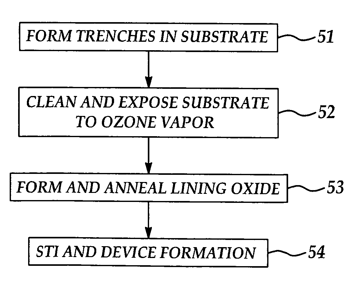
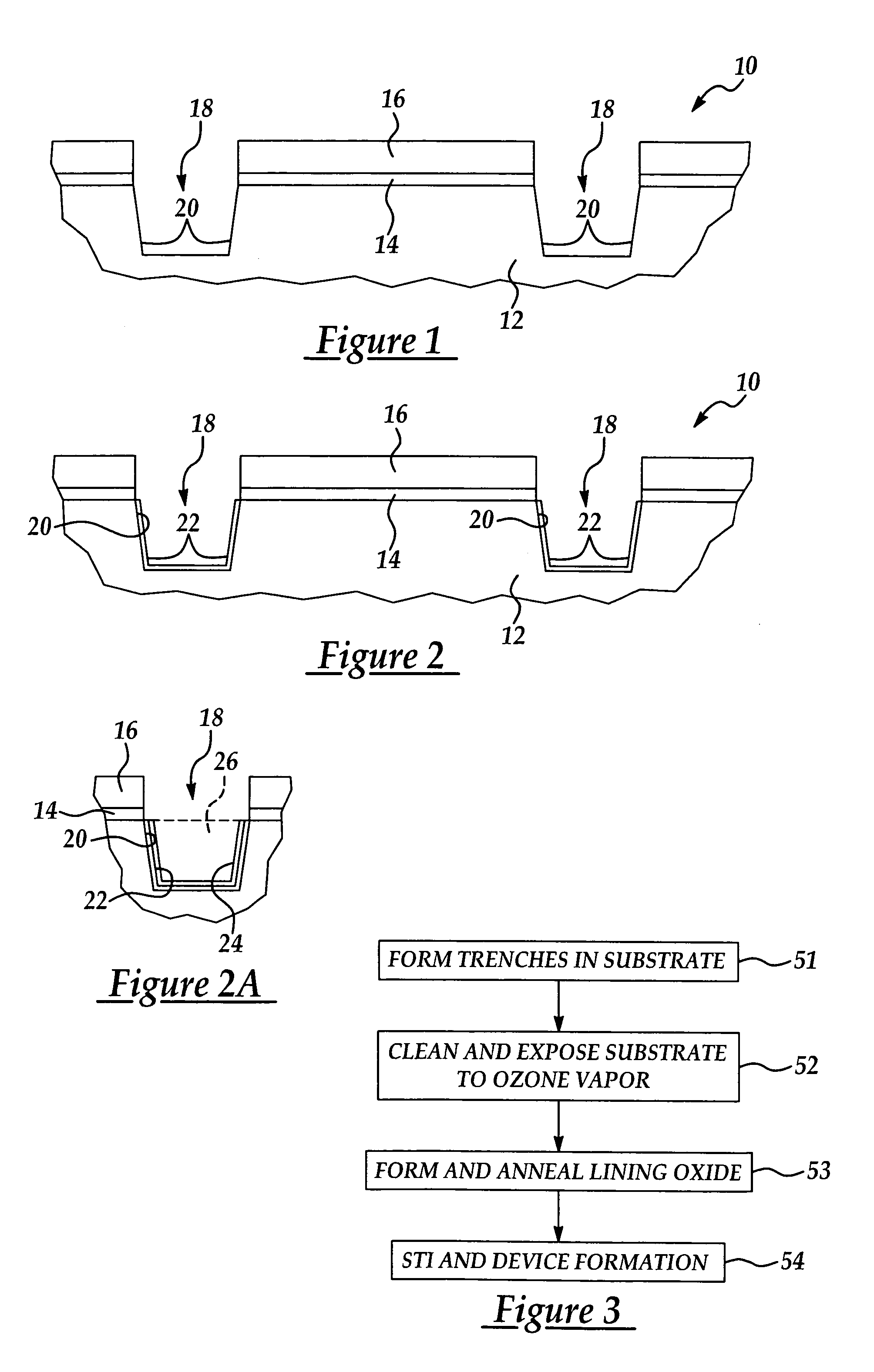
[0028]The present invention has particularly beneficial utility in the formation of a pre-liner oxide film on silicon surfaces in a trench etched into a substrate for the fabrication of STI (shallow trench isolation) structures on the substrate. However, the invention is not so limited in application, and while references may be made to such STI structures, the present invention is more generally applicable to forming an oxide film on a substrate in a variety of semiconductor fabrication applications, as well as applications in other industries.

[0029]The present invention includes a new and improved method for cleaning a substrate and forming a thin oxide layer or film on the substrate. The invention is suitably adapted for forming an oxide layer or film on a silicon surface. The method may be used to form a thin oxide film of high quality and uniform thickness on a silicon surface in the fabrication of semiconductor integrated circuits on a wafer substrate.

[0030]In the fabrication ...


PUM


Abstract

A method for cleaning and forming an oxide film on a surface, particularly a silicon surface. The surface is initially cleaned and then exposed to ozone vapor, which forms the oxide film on the surface. The method is particularly useful for forming a pre-liner oxide film on trench surfaces in the fabrication of STI (shallow trench isolation) structures.

Description

FIELD OF THE INVENTION[0001]The present invention relates to methods for cleaning semiconductor wafer substrates in the fabrication of integrated circuits. More particularly, the present invention relates to a method for cleaning substrates which includes exposing the substrates to ozone vapor to facilitate the growth of a thin, high-quality oxide layer on the substrates.BACKGROUND OF THE INVENTION[0002]The fabrication of various solid state devices requires the use of planar substrates, or semiconductor wafers, on which integrated circuits are fabricated. The final number, or yield, of functional integrated circuits on a wafer at the end of the IC fabrication process is of utmost importance to semiconductor manufacturers, and increasing the yield of circuits on the wafer is the main goal of semiconductor fabrication. After packaging, the circuits on the wafers are tested, wherein non-functional dies are marked using an inking process and the functional dies on the wafer are separat...

Claims


Application Information

Patent Timeline
Patent Type & Authority Patents(United States)
IPC IPC(8): H01L21/76H01L21/306H01L21/31H01L21/316H01L21/469H01L21/762
CPCH01L21/02057H01L21/02238H01L21/02255H01L21/76224H01L21/02307H01L21/31662H01L21/02304
Inventor CHENG, CHUNG-LONGTHEI, KONG-BENGKAO, JUNG-HUI
Owner TAIWAN SEMICON MFG CO LTD
Why Eureka
Try Eureka