Cleaning method and solution for cleaning a wafer in a single wafer process

a cleaning solution and cleaning method technology, applied in the field of semiconductor processing, can solve the problems of not being able to perform sc1/b>, affecting reducing the efficiency of cleaning, so as to minimize the process time and improve the effect of processing efficiency and efficient removal of aluminum and iron contamination

Inactive Publication Date: 2006-03-16
APPLIED MATERIALS INC
View PDF54 Cites 81 Cited by
  • Summary
  • Abstract
  • Description
  • Claims
  • Application Information

AI Technical Summary

Benefits of technology

[0011] The present invention is a method of use of a novel cleaning solution in a single wafer cleaning process. According to the present invention the method involves using a cleaning solution in a single wafer mode and the cleaning solution comprises at least ammonium hydroxide (NH4OH), hydrogen peroxide (H2O2), water (H2O) and a chelating agent. In an embodiment of the present invention the cleaning solution also contains a surfactant. In another embodiment of the present invention the cleaning solution also includes a dissolved gas such as H2. The same cleaning solution containing ammonium hydroxide, hydrogen peroxide, a chelating agent, and/or a surfactant and/or d...

Problems solved by technology

The SC1 solution, however, leaves metallic contaminants behind.
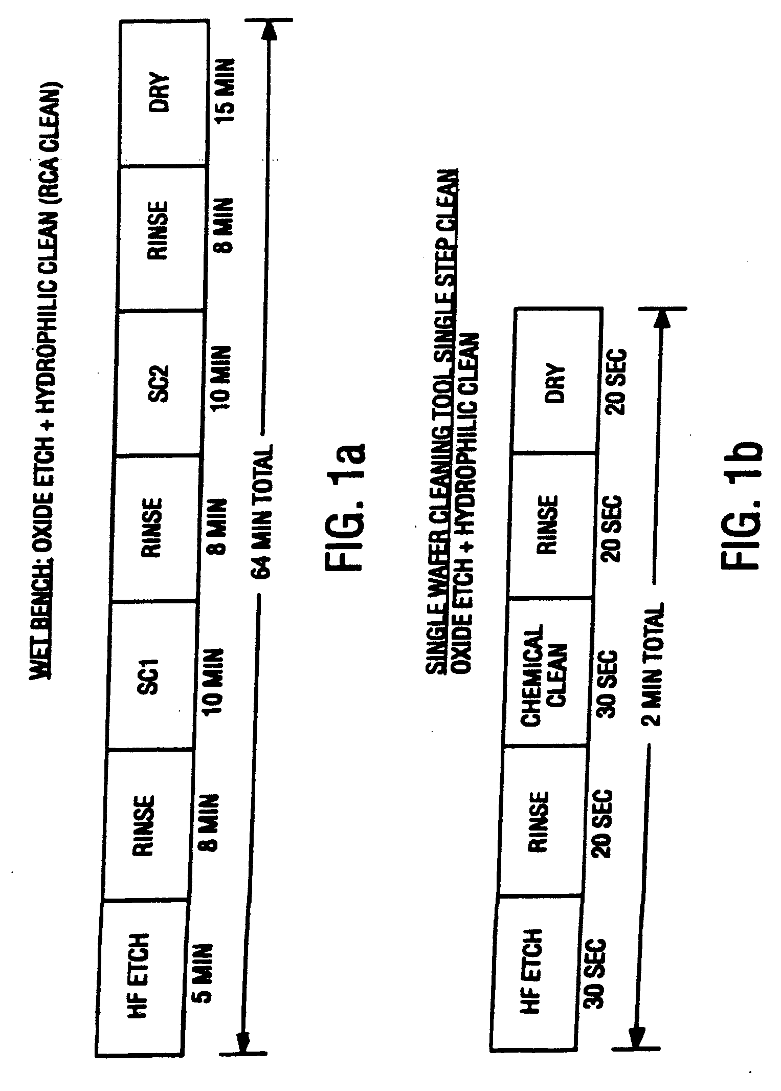
Usually the rate limiting step is the dryer which takes up to 15 min.
Unfortunately, presently it is not possible to perform an SC1-SC2 cleaning sequence in less than two minutes and at least within three minutes.
Until now, wet processing is usually done in a batch mode, since the throughput of singl...

Method used


Image

  • Cleaning method and solution for cleaning a wafer in a single wafer process
  • Cleaning method and solution for cleaning a wafer in a single wafer process
  • Cleaning method and solution for cleaning a wafer in a single wafer process

Examples


first embodiment

[0055] the present invention where the use of the single wafer cleaning tool and process is particularly useful is a combination of using hydrofluoric acid (HF) to strip an oxide surface of a wafer and using the modified cleaning solution as described above to clean the wafer in less than two minutes. This application is illustrated by a flow-chart in FIG. 8. In the first step 800 the wafer is placed in the single wafer cleaning tool. A substrate or wafer requiring cleaning is clamped face up to wafer support 610. Next, the wafer is subjected to an HF step 810. During the HF step 810 the wafer is spun at a rate between 10-2000 rpm, and preferably 100-1000 rpm, as diluted HF is fed through nozzle 614 and sprayed onto the top surface of wafer 608 to form an HF solution cover 622 over the entire front side of wafer 608. The HF solution may have a concentration in the range of 5-1000 parts water to one part HF. The HF solution is comprised of preferably 50 parts DI water to one part HF....

second embodiment

[0067] the current invention, shown in FIG. 9 in flow chart form, is a process which can be used to make the surface of the wafer hydrophobic. Instead of performing the HF step and then the chemical cleaning step, as set forth in FIG. 8, this process places the cleaning step before the HF step. Performing the HF step after the cleaning step leaves the surface of the wafer hydrophobic at the end of the cleaning process. All of the same details as described above with respect to FIG. 8 apply to the respective steps in the current process. The wafer is first placed in the single wafer cleaning tool by clamping the wafer face up to wafer support 610 (step 900.) The wafer is then spun as described above. The cleaning solution of the present invention, that optionally contains a cavitation gas, is then fed through nozzle 614 onto the top surface of wafer 608 as set forth in chemical cleaning step 910. Next, the wafer is rinsed in step 920 with a rinse that optionally contains an oxidant a...

third embodiment

[0068] the present invention, as shown in the flow chart in FIG. 11, is the use of the single wafer cleaning tool after an O2 ashing of the wafer to remove a photoresist. Most O2 plasma ashing steps are carried out in a single wafer mode and it is therefore very useful to have a single wafer cleaning method instead of a batch cleaning method after a O2 plasma ashing step. All of the same details as described above apply to the respective steps in the current process. The most significant difference in this process compared to the others disclosed in the present invention is that there is no HF step. There is no HF step is because the oxide surface on the wafer is needed in subsequent processing. In this application, after the O2 ashing step 1100, a wafer having an outer oxide film on a silicon surface is placed in the single wafer cleaning tool face up as described above and the wafer is spun. Next, as set forth in chemical cleaning step 1110, the wafer is cleaned with the cleaning ...


PUM

PropertyMeasurementUnit
Timeaaaaaaaaaa
Timeaaaaaaaaaa
Forceaaaaaaaaaa

Abstract

The present invention is a method of use of a novel cleaning solution in a single wafer cleaning process. According to the present invention the method involves using a cleaning solution in a single wafer mode and the cleaning solution comprises at least ammonium hydroxide (NH4OH), hydrogen peroxide (H2O2), water (H2O) and a chelating agent. In an embodiment of the present invention the cleaning solution also contains a surfactant. Moreover, the present invention also teaches a method of combining an ammonia hydroxide, hydrogen peroxide, and chelating agent step with a short HF step in a fashion that minimizes process time in a way that the entire method removes aluminum and iron contamination efficiently without etching too much oxide. The single wafer cleaning processes may also be used to increase the yield of high-grade reclaimed wafers.

Description

BACKGROUND OF THE INVENTION [0001] This application claims the benefit of U.S. Provisional Application No. 60 / 214,116 filed Jun. 26, 2000 and is a Continuation-in-Part of U.S. application Ser. No. 09 / 891,730 filed Jun. 25, 2001 entitled CLEANING METHOD AND SOLUTION FOR CLEANING A WAFER IN A SINGLE WAFER PROCESS.BACKGROUND OF THE INVENTION [0002] 1. Field of the Invention [0003] The present invention relates to the field of semiconductor processing and more specifically to a cleaning solution and a method of using the cleaning solution in a single wafer cleaning process. [0004] 2. Discussion of Related Art [0005] Wet etching and wet cleaning of silicon wafers is usually done by immersing silicon wafers into a liquid. This is also sometimes done by spraying a liquid onto a batch of wafers. Wafer cleaning and etching is traditionally done in a batch mode where several wafers (e.g. 50-100 wafers) are processed simultaneously. A typical cleaning sequence consists of HF-SC1-SC2. HF (Hydro...

Claims


Application Information

Patent Timeline
IPC IPC(8): B08B3/12C23G1/00B08B3/00C11D1/72C11D1/29C11D3/02C11D3/04C11D3/30C11D3/32C11D3/33C11D3/39C11D7/06C11D7/18C11D7/26C11D7/32C11D11/00H01L21/00H01L21/304H01L21/306
CPCC11D1/29C11D1/72C11D3/044C11D3/32C11D3/33H01L21/67051C11D7/06C11D7/265C11D11/0047H01L21/02052C11D3/3947
Inventor RAYANDAYAN, RONALDVERHAVERBEKE, STEVENWANG, HONG
Owner APPLIED MATERIALS INC
Why Eureka
Try Eureka