Ferroelectric capacitor stack etch cleaning methods

a technology of ferroelectric capacitors and etching, which is applied in the direction of capacitors, basic electric elements, electrical appliances, etc., can solve the problems of achieve the effect of reducing capacitor leakage and other performance degradation, reducing ferroelectric material damage and capacitor leakag

Active Publication Date: 2006-06-22
TEXAS INSTR INC
View PDF19 Cites 71 Cited by
  • Summary
  • Abstract
  • Description
  • Claims
  • Application Information

AI Technical Summary

Benefits of technology

[0005] The following presents a simplified summary in order to provide a basic understanding of one or more aspects of the invention. This summary presents one or more concepts of the invention in a simplified form as a prelude to the more detailed description that is presented later and is not an extensive overview of the invention. In this regard, the summary is not intended to identify key or critical elements of the invention, nor does the summary delineate the scope of the invention. Etching processes used for patterning the ferroelectric cell capacitor stack structures can lead to damage of the ferroelectric material. The inventors have found that while conventional post-etch cleaning operations may help to mitigate ferroelectric material damage and capacitor leakage, these issues remain a problem in the fabrication of semiconductor devices employing ferroelectric capacitors, particularly capacitor leakage where the sizes thereof are scaled to smaller and smaller dimensions. The present invention relates to semiconductor fabrication techniques in which etched ferroelectric capacitor structures are cleaned prior to forming an overlying dielectric (ILD) material. Methods are provided for fabricating a ferroelectric capacitor structure, and for etching and cleaning patterned ferroelectric capacitor structures in a semiconductor device, by which capacitor leakage and other performance degradation may be mitigated.

Problems solved by technology

Etching processes used for patterning the ferroelectric cell capacitor stack structures can lead to damage of the ferroelectric material.
The inventors have found that while conventional post-etch cleaning operations may help to mitigate ferroelectric material damage and capacitor leakage, these issues remain a problem in the fabrication of semiconductor devices employing ferroelectric capacitors, particularly capacitor leakage where the sizes thereof are scaled to smaller and smaller dimensions.

Method used


Image

  • Ferroelectric capacitor stack etch cleaning methods
  • Ferroelectric capacitor stack etch cleaning methods
  • Ferroelectric capacitor stack etch cleaning methods

Examples


Embodiment Construction

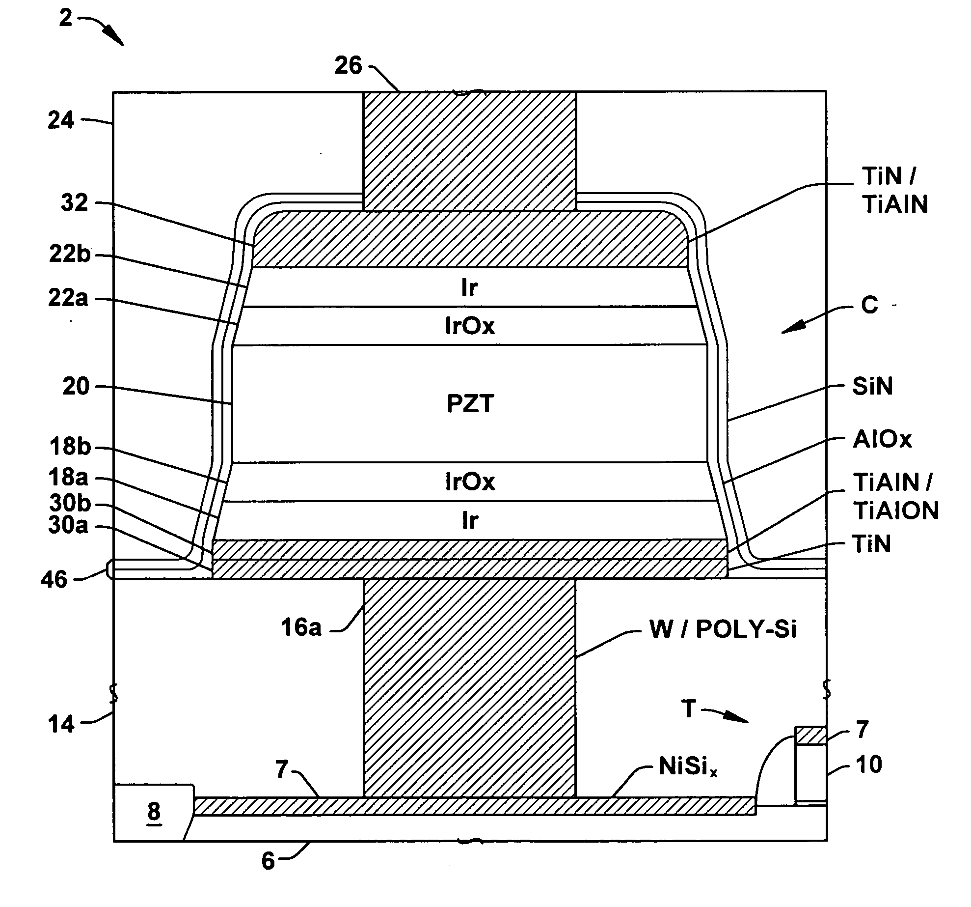
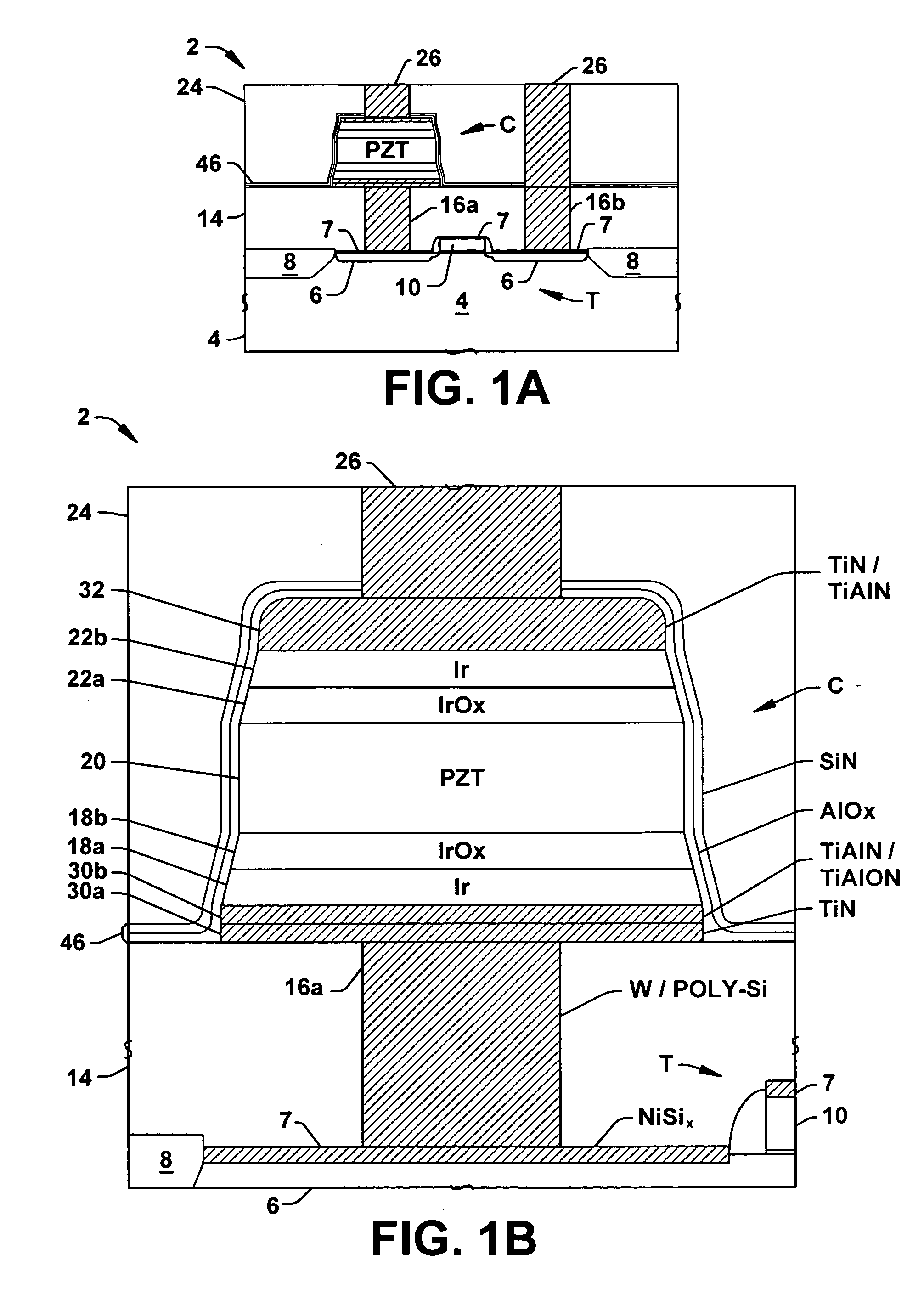
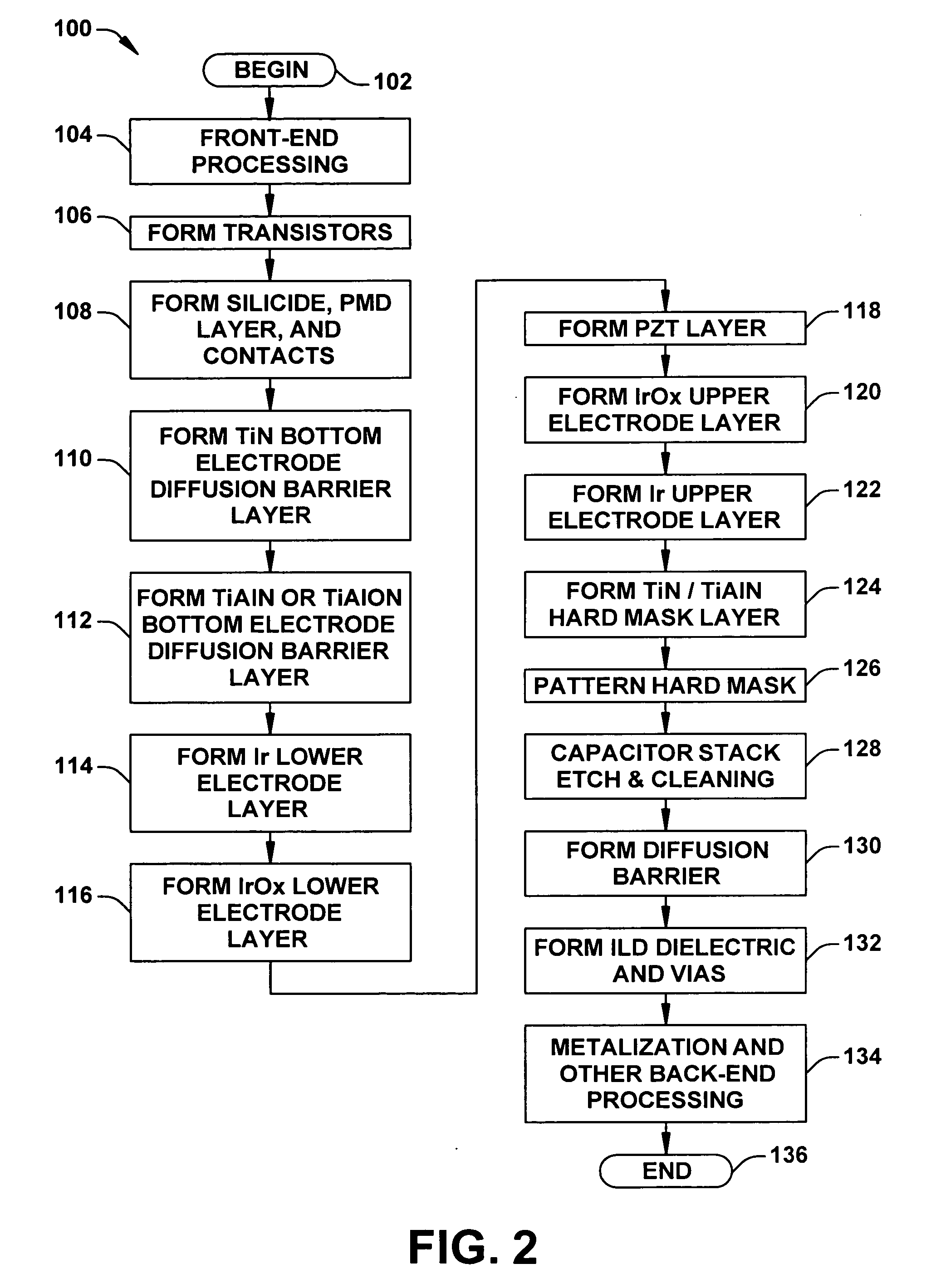
[0016] The present invention will now be described with reference to the attached drawing figures, wherein like reference numerals are used to refer to like elements throughout. The invention relates to the use of high temperature ashing processes and wet cleaning of etched ferroelectric capacitor stack structures, by which capacitor leakage may be mitigated in the fabrication of semiconductor devices. The invention may be carried out in any type of semiconductor device, for example, devices having memory cells with ferroelectric cell capacitors or other devices, such as integrated circuits, in which ferroelectric capacitors are used. The various aspects and advantages of the invention are hereinafter illustrated and described in conjunction with the drawings, wherein the illustrated structures are not necessarily drawn to scale.

[0017]FIGS. 1A and 1B illustrate an exemplary ferroelectric memory cell (1T1C) with a cell transistor T and a ferroelectric capacitor C in a semiconductor ...


PUM


Abstract

Methods (100) are provided for fabricating a ferroelectric capacitor structure including methods (128) for etching and cleaning patterned ferroelectric capacitor structures in a semiconductor device. The methods comprise etching (140, 200) portions of an upper electrode, etching (141, 201) ferroelectric material, and etching (142, 202) a lower electrode to define a patterned ferroelectric capacitor structure, and etching (143, 206) a portion of a lower electrode diffusion barrier structure. The methods further comprise ashing (144, 203) the patterned ferroelectric capacitor structure using a first ashing process, performing (145, 204) a wet clean process after the first ashing process, and ashing (146, 205) the patterned ferroelectric capacitor structure using a second ashing process directly after the wet clean process at a high temperature in an oxidizing ambient.

Description

FIELD OF INVENTION [0001] The present invention relates generally to semiconductor devices and more particularly to methods for cleaning etched ferroelectric capacitor structures in the fabrication of semiconductor devices. BACKGROUND OF THE INVENTION [0002] Memory systems are used for storage of data, program code, and / or other information in many electronic products, such as personal computer systems, embedded processor-based systems, video image processing circuits, portable phones, and the like. Ferroelectric memory, sometimes referred to as “FRAM” or “FERAM”, is a non-volatile form of memory commonly organized in single-transistor, single-capacitor (1T1C) or two-transistor, two-capacitor (2T2C) cell configurations, in which each memory cell includes one or more pairs of access transistors and cell capacitors formed using ferroelectric dielectric material. The non-volatility of an FERAM memory cell results from a bi-stable or multi-stable characteristic of the ferroelectric diel...

Claims


Application Information

Patent Timeline
Patent Type & Authority Applications(United States)
IPC IPC(8): H01L21/00
CPCH01L21/0206H01L21/02071H01L28/55H01L28/57H01L28/65H01L28/75
Inventor SUMMERFELT, SCOTT R.HALL, LINDSEY H.UDAYAKUMAR, K. R.MOISE, THEODORE S. IV
Owner TEXAS INSTR INC
Why Eureka
Try Eureka