Integrated circuit device

Inactive Publication Date: 2007-01-02
TESSERA TECH HUNGARY KFT +1
View PDF46 Cites 53 Cited by
  • Summary
  • Abstract
  • Description
  • Claims
  • Application Information

AI Technical Summary

Benefits of technology

[0024]an integrated circuit die containing at least one of a radiation emitter and radiation receiver and having top and bottom surfaces formed of electrically insulative and mechanically protective material, at least one of the surfaces being transparent to radiation, the integrally packaged optronic integrated circuit device being characterized in that its longest dimension does not exceed the longest d

Problems solved by technology

Both wire bonding and TAB bonding are prone to bad bond formation and subject the die to relatively high temperatures and mechanical pressures.
Both wire bond and TAB technologies are problematic from a package size viewpoint, producing integrated circuit devices having a die-to-package area ratio ranging from about 10% to 60%.
The

Method used


Image

  • Integrated circuit device
  • Integrated circuit device
  • Integrated circuit device

Examples


Embodiment Construction

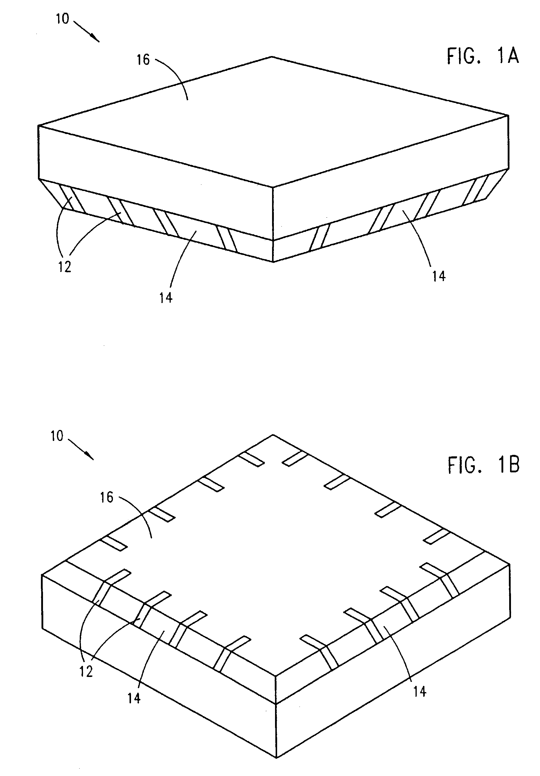
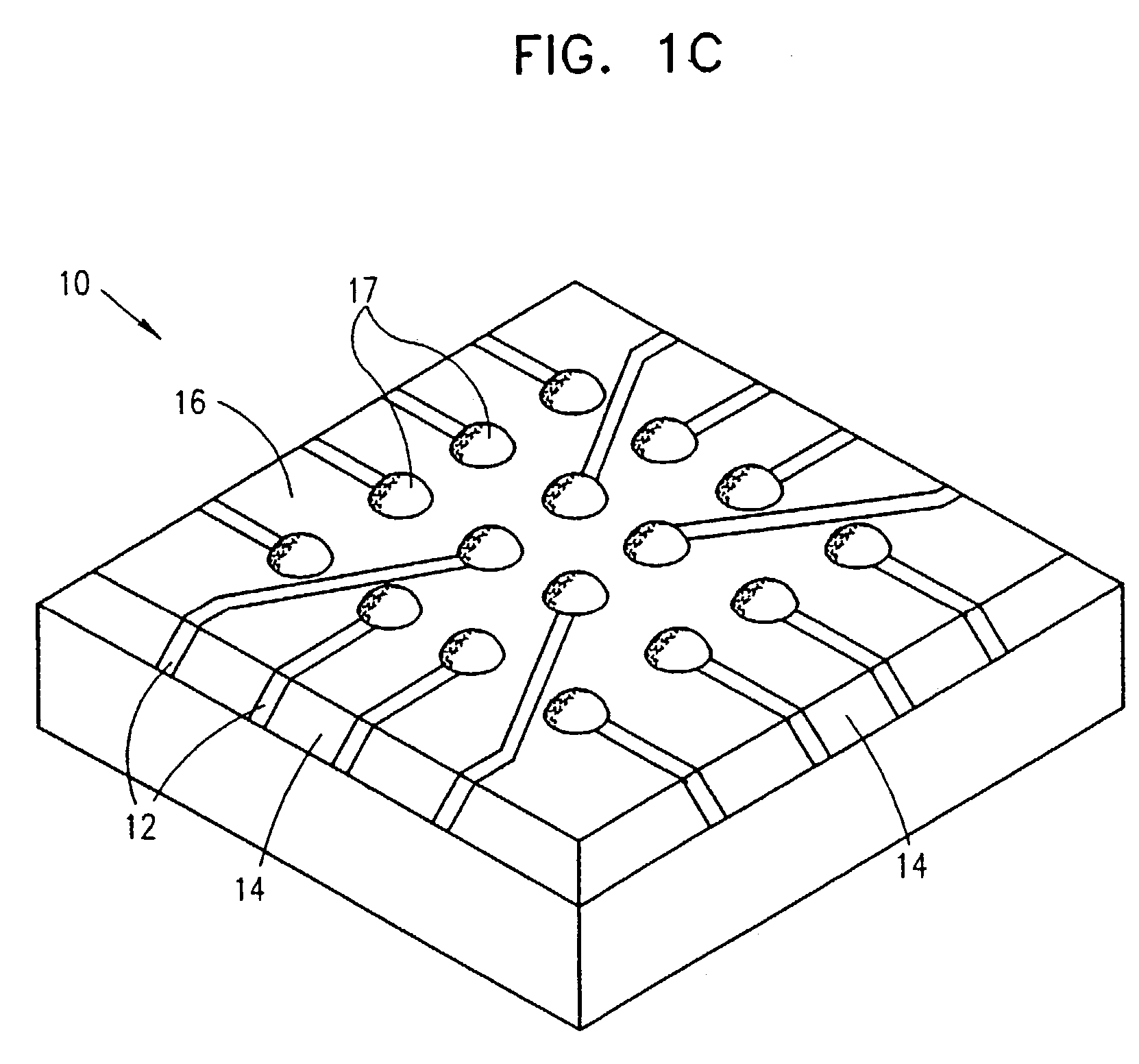
[0051]Reference is now made to FIGS. 1A–22, which illustrate the production of integrated circuit devices in accordance with a preferred embodiment of the present invention.

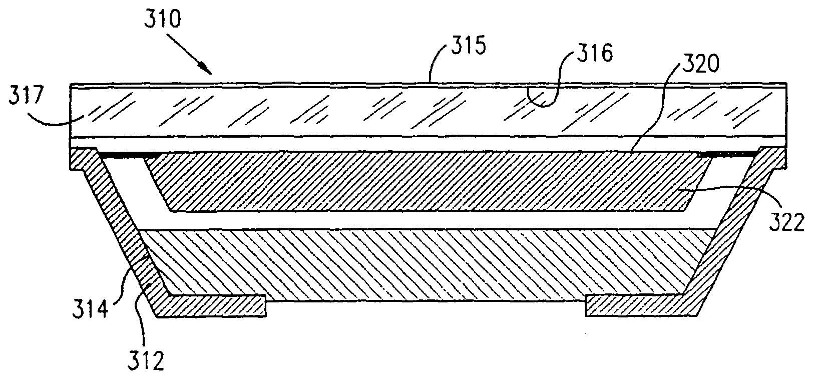
[0052]FIGS. 1A and 1B together illustrate a preferred embodiment of integrated circuit device constructed and operative in accordance with a preferred embodiment of the present invention. The integrated circuit device includes a relatively thin and compact, environmentally protected and mechanically strengthened integrated circuit package 10 having a multiplicity of electrical contacts 12 plated along the edge surfaces 14 thereof.

[0053]In accordance with a preferred embodiment of the invention, contacts 12 extend over edge surfaces onto the planar surfaces 16 of the, package. This contact arrangement permits both flat surface mounting and edge mounting of package 10 onto a circuit board. It is noted that the integrated circuit package 10 may include one or more of the following elements (not shown): an integrally...


PUM


Abstract

An integrally packaged optronic integrated circuit device (310) including an integrated circuit die (322) containing at least one of a radiation emitter and radiation receiver and having top and bottom surfaces formed of electrically insulative and mechanically protective material, at least one of the surfaces (317) being transparent to radiation, and electrically insulative edge surfaces (314) having pads.

Description

[0001]This application is a continuation of patent application Ser. No. 09 / 601,895 filed on Sep. 22, 2000, now U.S. Pat. No. 6,646,289 which is a 371 of International Application PCT / IL99 / 00071, filed on 3 Feb. 1999, and which has designated the U.S., which claims priority to Israeli Patent Application No. 123207 filed Feb. 6, 1998.FIELD OF THE INVENTION[0002]The present invention relates to methods and apparatus for producing integrated circuit devices and to integrated circuit devices produced thereby and more particularly to an optronic integrally packaged die.BACKGROUND OF THE INVENTION[0003]An essential step in the manufacture of all integrated circuit devices is known as “packaging” and involves mechanical and environmental protection of a silicon chip which is at the heart of the integrated circuit as well as electrical interconnection between predetermined locations on the silicon chip and external electrical terminals.[0004]At present three principal technologies are employ...

Claims


Application Information

Patent Timeline
IPC IPC(8): H01L27/15H01L29/22H01L29/267H01L31/12H01L33/00H01L23/31H01L23/485H01L25/10H01L27/146H01L31/02H01L33/58H01L33/62
CPCH01L23/3114H01L33/52H01L24/97H01L27/14618H01L27/14632H01L27/14687H01L27/15H01L31/0203H01L31/0232H01L24/02H01L25/105H01L33/486H01L33/62H01L2224/0401H01L2924/01005H01L2924/01006H01L2924/01014H01L2924/01027H01L2924/01029H01L2924/01033H01L2924/01051H01L2924/01057H01L2924/01077H01L2924/01078H01L2924/01079H01L2924/014H01L2924/14H01L2924/10253H01L2924/01068H01L2924/00H01L31/02327H01L24/24H01L2224/24225H01L2224/24051H01L2224/94H01L2224/97H01L24/82H01L2224/82H01L23/02H01L21/56H01L21/82H01L31/02002H01L31/02164H01L31/125H01L31/186H01L33/0095H01L33/44H01L33/483H01L33/56H01L2221/68327
Inventor BADEHI, AVNER
Owner TESSERA TECH HUNGARY KFT
Why Eureka
Try Eureka