

Repairable block redundancy scheme
a redundancy scheme and repairable technology, applied in error prevention, digital transmission, instruments, etc., can solve the problems of limited number of defective main memory blocks, unreliability or some way defective parts of memory arrays, and certain portions of memory arrays
- Summary
- Abstract
- Description
- Claims
- Application Information
AI Technical Summary
Benefits of technology
Problems solved by technology
Method used
Image

Examples
Embodiment Construction
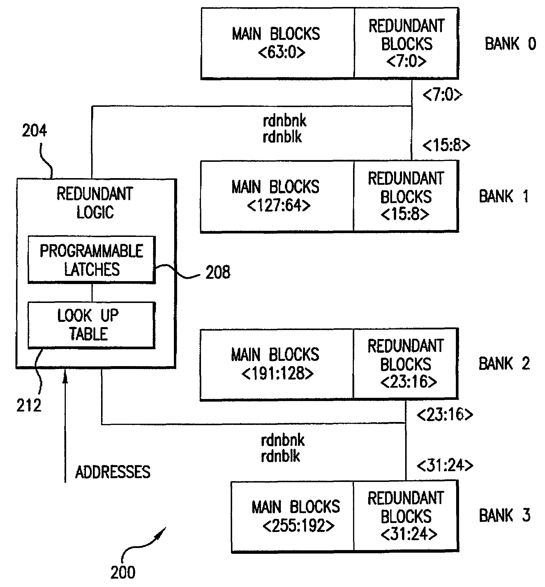
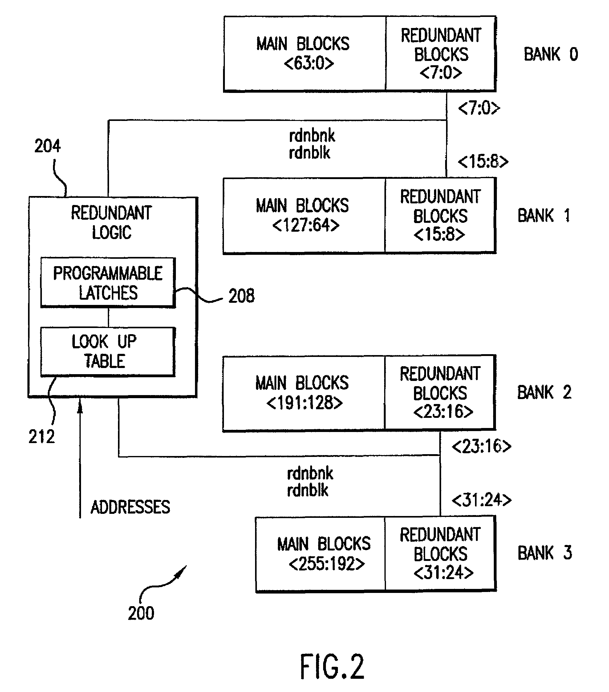
[0018]The present invention can generally be used to substitute one memory block for another memory block and particularly may be used for substituting a non-defective memory block for a defective memory block within a memory system. It is particularly useful in non-volatile memory systems such as flash memory.
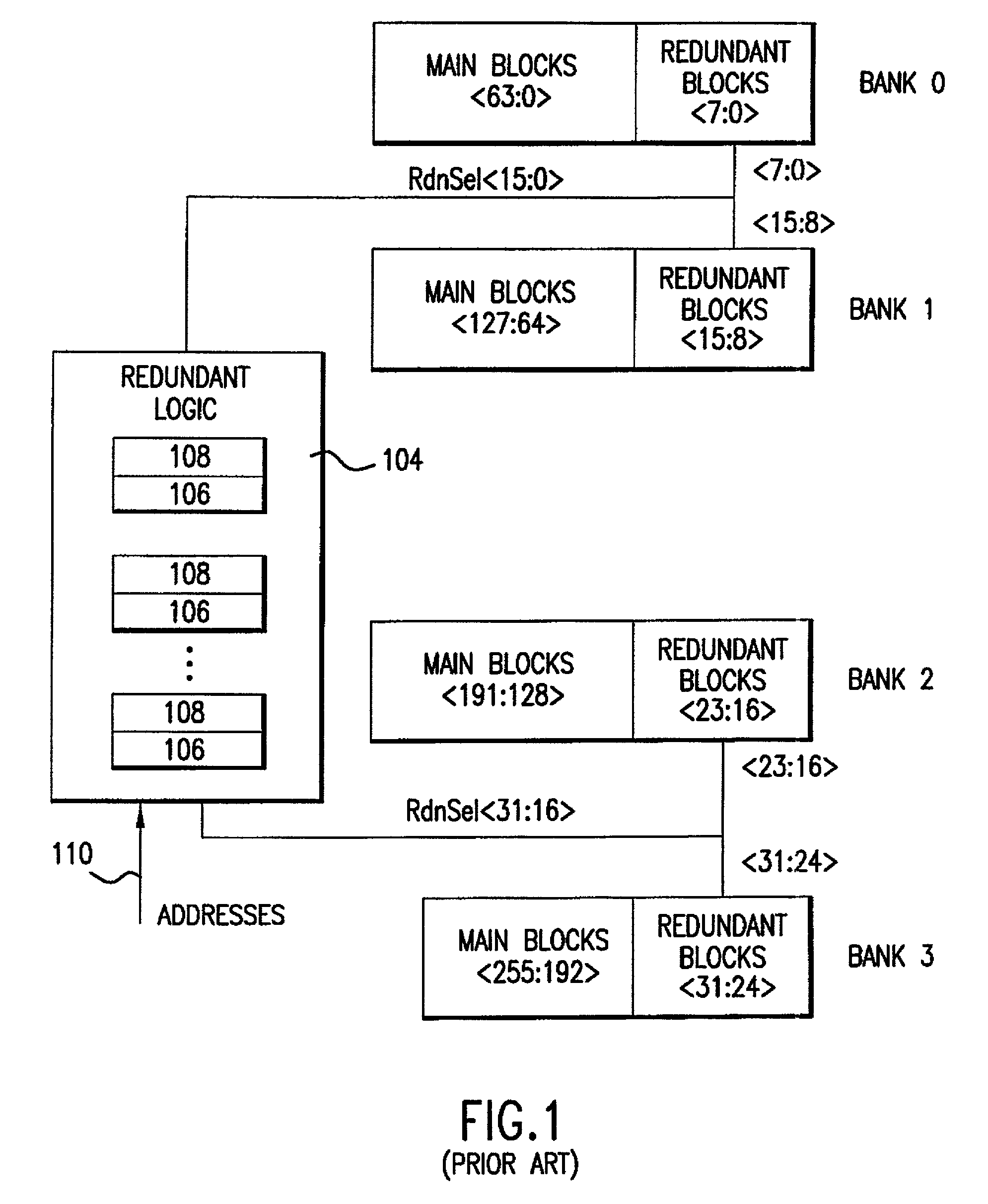
[0019]As shown in FIG. 1, it is known to divide a memory device such as flash memory into memory banks and to further divide the memory banks into memory blocks. FIG. 1 shows memory banks 0–3 each having 64 main memory blocks and 8 redundant memory blocks contained therein. Thus, bank 0 contains main memory blocks addressable as 63:0> and redundant memory blocks addressable as 7:0>, while memory banks 1–3 respectively contain memory blocks 127:64>, redundant blocks 15:8>, main blocks 191:128>, redundant blocks 23:16>, and main blocks 255:192>, and redundant blocks 31:24> respectively. In FIG. 1 all of the main memory blocks and redundant blocks are of the same size. It should ...
PUM
 Abstract
Description
Claims
Application Information