

Load sensor and method of manufacturing the load sensor, paste used for the method, and method of manufacturing the paste
a technology of load sensor and manufacturing method, applied in the direction of resistor details, superconductor devices, instruments, etc., can solve the problems of difficult use when high reliability and strength are required, the strength and layer quality of alkoxide is lower, and the surface roughens, etc., to achieve the effect of reducing manufacturing cost and easy formation of multiple layers of wiring
- Summary
- Abstract
- Description
- Claims
- Application Information
AI Technical Summary
Benefits of technology
Problems solved by technology
Method used
Image

Examples
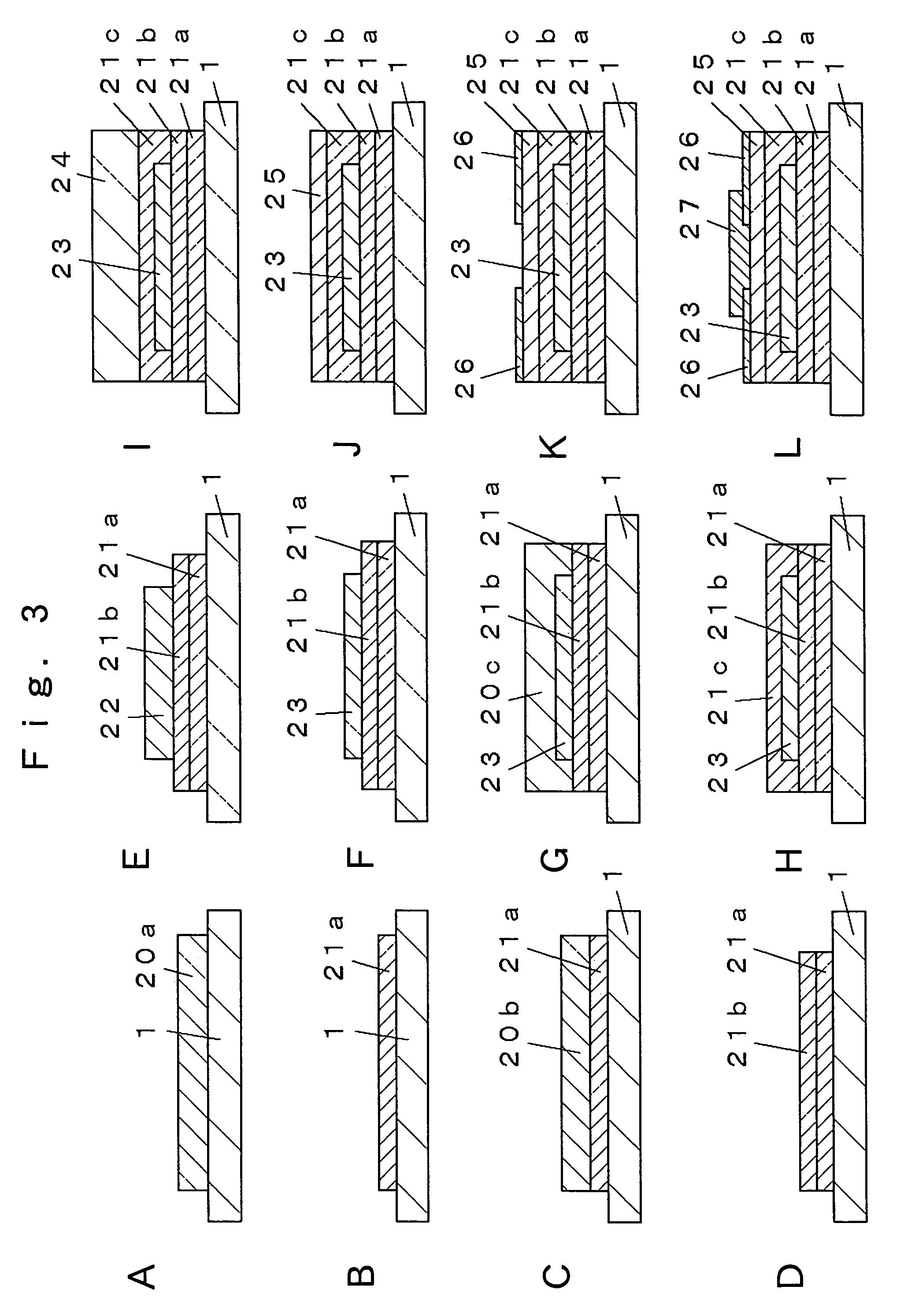
embodiment 1
(Preferred Embodiment 1)
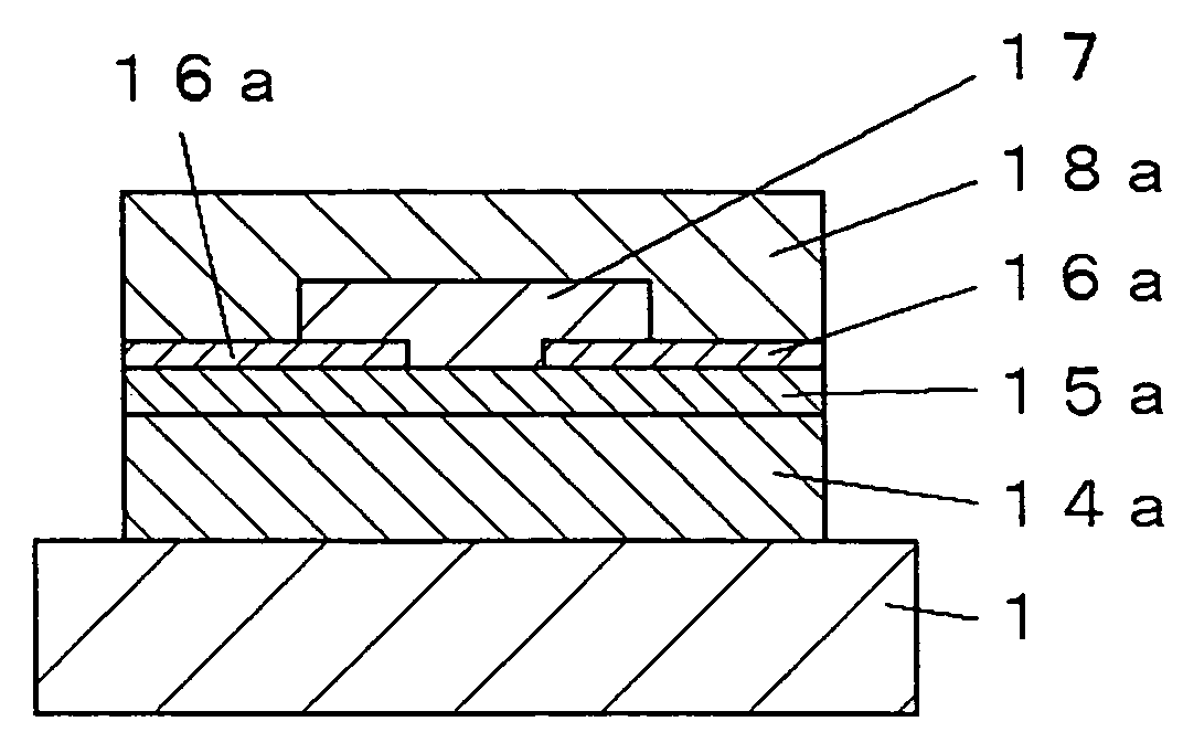
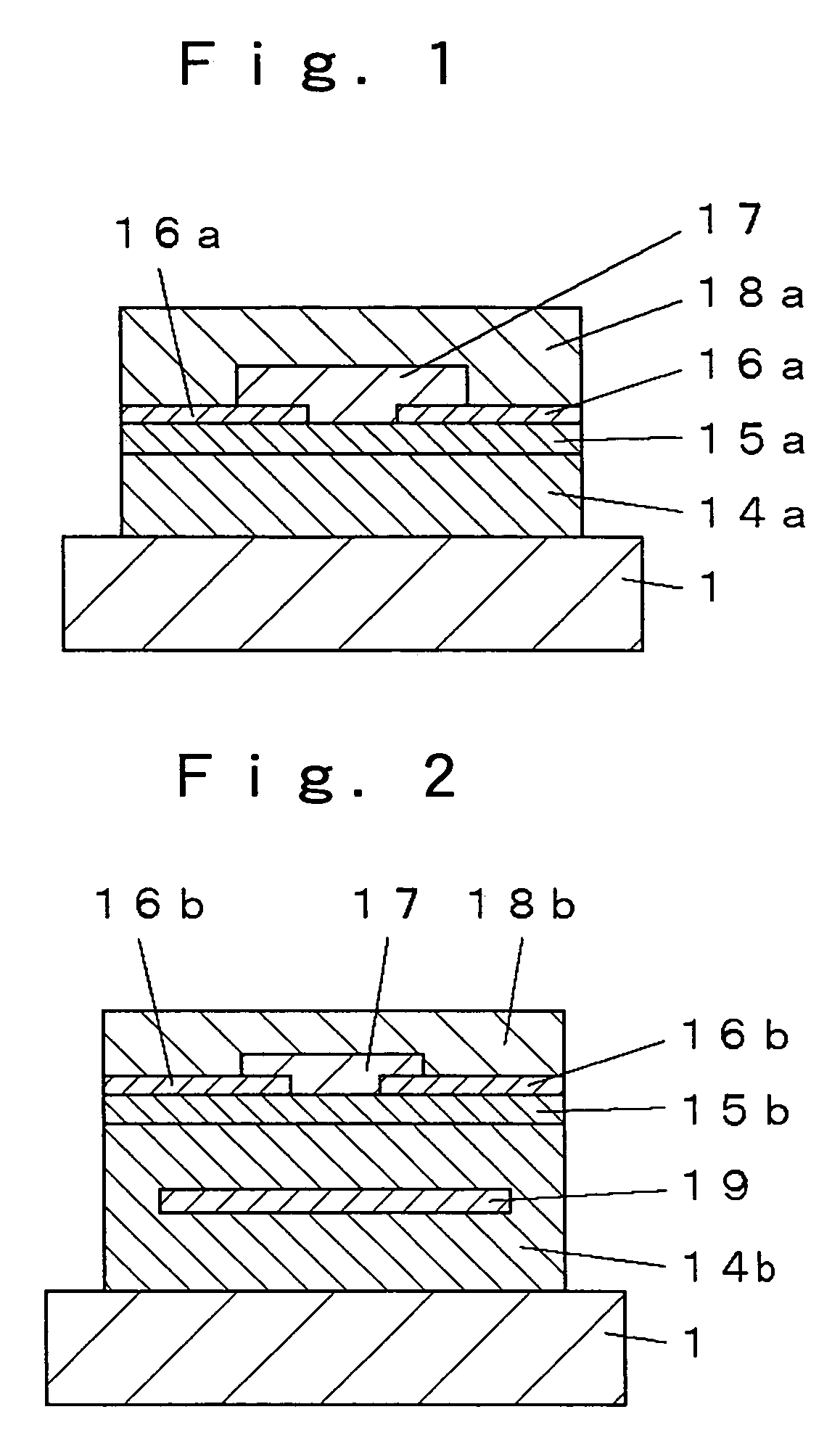
[0057]A load sensor with multi-layer wiring will be described with reference to FIG. 1 and FIG. 2. FIG. 1 is a sectional view of a load sensor with single-layer wiring. FIG. 2 is a sectional view of a load sensor with multi-layer wiring. In FIG. 1, crystallized glass 14a is formed on elastic metal body 1, on which wiring 16a and strain sensitive resistor 17 are formed via non-crystalline glass 15a, and protective layer 18a is formed in such manner that at least the strain sensitive resistor 17 is buried therein.
[0058]Also, in FIG. 2, crystallized glass 14b with internal electrode 19 built therein is formed on the elastic metal body 1, on which wiring 16b and strain sensitive resistor 17 are further formed via non-crystalline glass 15b, and protective layer 18b is formed in such manner that at least the strain sensitive resistor 17 is buried therein.
[0059]Incidentally, FIG. 2 is different from FIG. 2 in such point that the internal electrode 19 is built into t...
embodiment 2
(Preferred Embodiment 2) Composition of Non-Crystalline Glass
[0086]In the preferred embodiment 2, multi-layer wiring and optimization of non-crystalline glass being able to cope with simultaneous burning with crystalline glass will be described.
[0087]First, as shown by composition No. 1 to 5 in Table 5, SiO2 was reduced to shift the composition with respect to CaO, ZrO2, Al2O3, and B2O3, but excellent results were not obtained. Accordingly, as shown by composition No. 6 to 10 in Table 5, the amount of SiO2 was adjusted to 45 to 65 wt % to shift the composition with respect to CaO, ZrO2, PbO, Al2O3, and B2O3, then excellent results were obtained. On the other hand, as shown by composition No. 11 to 14 in Table 5, when the amount of SiO2 was adjusted to 70 wt % or over, excellent results were no obtained.
[0088]
TABLE 5CompositionComposition (weight part)SurfaceHeatTotalNo.SiO2CaOZrO2PbOAl2O3roughnessresistanceMatchingevaluation1 0 to 100 to 200 to 200 to 200 to 20Δ◯ΔΔ210 to 200 to 200 ...
embodiment 3
(Preferred Embodiment 3) Optimization of Crystalline Glass
[0101]In the preferred embodiment 3, crystallized glass that can be simultaneously burnt is optimized also in combination with commercially available non-crystalline glass (for example, borosilicate lead-based B2O3—SiO2—PbO).
[0102]Table 8 is an example of optimization of crystalline glass composition. Table 8 shows the compositions with the rate of MgO shifted. As a result, it has been found that the rate is desirable to be 30 to 55 wt % because the rate of MgO is mutually related with crystallinity. As shown in Table 9, Table 10 and Table 11, optimization has been executed with respect to SiO2, B2O3, BaO, ZrO2, and Al2O3.
[0103]Consequently, it has been found that sintering property is improved by the addition of SiO2 and B2O3 and that the characteristic is improved by the addition of a specific amount of alumina. Also, the amount of CaO added is desirable to be 0 to 6 wt %. The surface roughens with increase in the amount of...
PUM
| Property | Measurement | Unit |
|---|---|---|
| thickness | aaaaa | aaaaa |
| thickness | aaaaa | aaaaa |
| thickness | aaaaa | aaaaa |
Abstract
Description
Claims
Application Information