Method of making thin silicon sheets for solar cells

a solar cell and silicon sheet technology, applied in the direction of sustainable manufacturing/processing, final product manufacturing, after-treatment details, etc., can solve the problems of not always the case, the cost of a starting silicon wafer is typically nearly half of the value of the finished photovoltaic module, and the photovoltaic solar cell industry is extremely cost sensitiv

Inactive Publication Date: 2007-01-30
AUSTRALIEN NAT UNIV
View PDF7 Cites 110 Cited by
  • Summary
  • Abstract
  • Description
  • Claims
  • Application Information

AI Technical Summary

Benefits of technology

[0015]Preferably, adjacent and opposing etch fronts meet to provide for separation of the layer of silicon which will no longer be joined to the substrate when the etch fronts meet. Alternatively, the etching proceeds until adjacent and opposing etch fronts almost meet and the layer of silicon is then mechanically detached by breaking of the remaining connection(s) between the layers and the substrate. Thus, by “substantially meet” is meant that the adjacent and opposing etch fronts approach each other sufficiently closely that the layer of silicon present above the lateral channels remains attached to the substrate but is readily removable from it.
[0024]It will be apparent that the present invention allows ordinary silicon wafers to be processed to produce thin rectangular strips of silicon or a silicon sheet, the thickness of the strips or the sheet being much smaller than the wafer thickness. The individual strips or sheet can be processed into solar cells and then detached from the substrate. Following this process, a layer of substrate is removed which is much thinner than can be achieved by prior art cutting processes, with much less waste than using prior art processes. Because the substrate has been reduced in thickness by an amount much less than the original substrate thickness, the remainder can be re-used for the production of further thin silicon strips or sheet. Thus, from a single silicon wafer it is possible to obtain at least two, and typically several, thin layers for use (for instance) in solar cells.

Problems solved by technology

However, this is not always the case.
For example, the photovoltaic solar cell industry is extremely cost sensitive, and the cost of a starting silicon wafer is typically nearly half of the value of the finished photovoltaic module.
However, the kerf loss in sawing the wafer is approximately 250 μm, meaning that most of the boule ends up as powder.

Method used


Image

  • Method of making thin silicon sheets for solar cells
  • Method of making thin silicon sheets for solar cells
  • Method of making thin silicon sheets for solar cells

Examples


Embodiment Construction

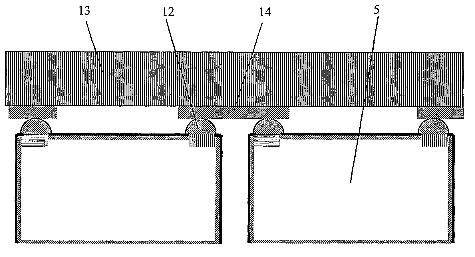
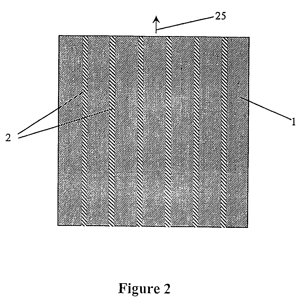
[0014]In the present invention, by “surface of a silicon substrate of substantially (111) orientation” is meant that the silicon substrate is either of precisely (111) orientation, or otherwise sufficiently close to (111) orientation that when the lateral channels have been etched, adjacent channels either meet or approach each other sufficiently closely that the layer may be detached from the substrate by the application of force substantially without damaging the layer. Typically the surface of the silicon substrate is at an angle of from 0° to about 10° from the (111) orientation, more typically from 0° to about 7°, more typically from 0° to about 40°.

[0015]Preferably, adjacent and opposing etch fronts meet to provide for separation of the layer of silicon which will no longer be joined to the substrate when the etch fronts meet. Alternatively, the etching proceeds until adjacent and opposing etch fronts almost meet and the layer of silicon is then mechanically detached by breaki...


PUM

PropertyMeasurementUnit
thicknessaaaaaaaaaa
angleaaaaaaaaaa
angleaaaaaaaaaa

Abstract

A thin layer of single-crystal silicon is produced by forming first trenches in a silicon substrate having (111) orientation; forming narrower second trenches at the bases of the trenches; anisotropically etching lateral channels (4) from the second trenches, until adjacent etch fronts (16) substantially meet; and detaching said layer from the substrate. The trenches may be arranged so that the resultant layer has rows of slots, whit the slots in adjacent rows being mutually offset. Solar cells may be formed on strips (5) between the trenches, having lengths of more than 50 mm, widths of up to 5 mm, and thicknesses of less than 100 microns, and having two electrical contacts on the same face (6) of each strip (5).

Description

[0001]This application is a 371 of PCT / AU02 / 01640 filed Dec. 4, 2002.FIELD OF THE INVENTION[0002]This invention relates to processes for producing thin crystalline layers of silicon, to the fabrication of solar cells from these layers, and to solar cells fabricated from these layers.BACKGROUND[0003]In most areas of semiconductor processing, the cost of the starting substrate wafer is small compared to the value of the final, processed wafer. However, this is not always the case. For example, the photovoltaic solar cell industry is extremely cost sensitive, and the cost of a starting silicon wafer is typically nearly half of the value of the finished photovoltaic module. Thus, in this industry it is extremely important that the silicon substrates are used as efficiently as possible. These substrates are produced by sawing thin slices from a cylindrical boule of crystalline silicon. The thinnest slice that can be cut is determined by the mechanical properties of the silicon and the sa...

Claims


Application Information

Patent Timeline
Patent Type & Authority Patents(United States)
IPC IPC(8): H01L21/336C30B33/00H01L21/306H01L31/04H01L31/05H01L31/18
CPCC30B29/06C30B33/00H01L21/30608H01L31/022425H01L31/0516H01L31/0682H01L31/1804Y10T428/2457Y02E10/547H01L31/022441Y02P70/50
Inventor BLAKERS, ANDREW WILLIAMWEBER, KLAUS JOHANNES
Owner AUSTRALIEN NAT UNIV
Why Eureka
Try Eureka