TDDB test pattern and method for testing TDDB of MOS capacitor dielectric
a dielectric and capacitor technology, applied in the direction of individual semiconductor device testing, semiconductor/solid-state device testing/measurement, instruments, etc., can solve the problem of high cost of testing equipment for a prolonged time period, and achieve the effect of improving the accuracy of the measurement result and reducing the measuring cos
- Summary
- Abstract
- Description
- Claims
- Application Information
AI Technical Summary
Benefits of technology
Problems solved by technology
Method used
Image
Examples
first embodiment
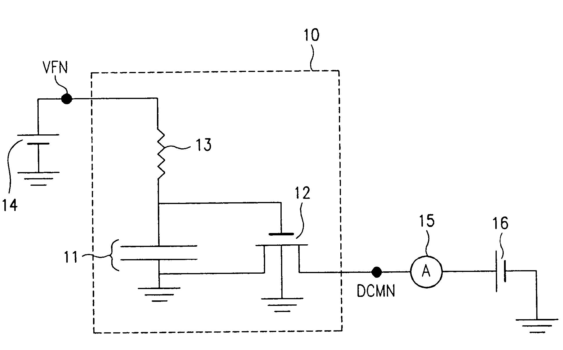
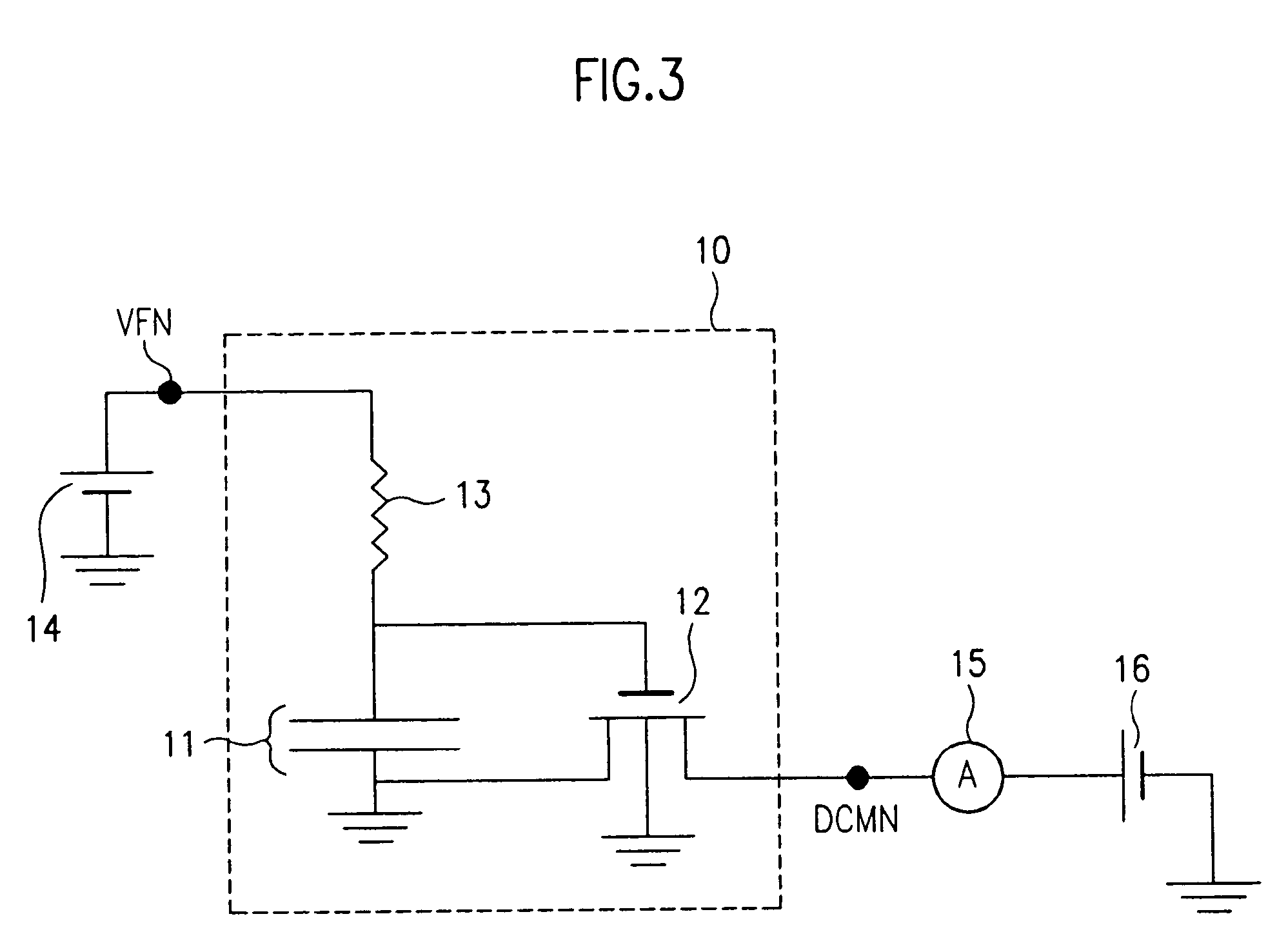
[0031]The TDDB test pattern of the present invention having the foregoing circuit will be explained with reference to embodiments of the present invention. FIG. 7 shows a first embodiment where a voltage stress is applied to a dielectric film in an MOS capacitor 11 in an inversion mode. In this case, the type of the MOS transistor 12 is the same type as the MOS capacitor 11. For example, as shown in FIG. 7, if the MOS capacitor 11 is an NMOS type, the MOS transistor 12 is also NMOS. And, when the voltage stress is to be applied in the inversion mode, additional source and drain is formed in the MOS capacitor 11.
second embodiment
[0032]FIG. 8 shows a second embodiment where the voltage stress is applied to a dielectric film in an MOS capacitor 11 in an accumulation mode. In this case, the type of the MOS transistor 12 should be that opposite to that of the MOS capacitor 11. For example, as shown in FIG. 8, if the MOS capacitor 11 is an NMOS type, the MOS transistor 12 should be PMOS transistor.
[0033]Also, as shown in FIGS. 7 and 8, the main test pattern includes four input / output pads including a substrate pad (not shown) for connecting the MOS capacitor 11 and a bulk electrode of the MOS transistor 12 in each unit test pattern cell, a source pad 117 for connecting source electrodes of the MOS transistors 12, a VFN pad 18 for connecting VFNs of unit test cells, and a DCMN pad 19 for connecting the DCMN connected to the drain electrode of the MOS transistor 12 in each unit test pattern cell. In the accumulation mode, two more pads are provided to be connected to the source and the drain of the MOS capacitor b...
PUM
 Abstract
Description
Claims
Application Information


