Method and system for wideband device measurement and modeling

a wideband device and wideband characteristics technology, applied in the direction of resistance/reactance/impedence, testing circuits, instruments, etc., can solve the problems of inability to meet the wideband, ultra high-frequency, high-speed, nonlinear design needs, and inability to accurately model the design

Inactive Publication Date: 2007-01-30
FRONTEND ANALOG & DIGITAL TECH CORP
View PDF2 Cites 26 Cited by
  • Summary
  • Abstract
  • Description
  • Claims
  • Application Information

AI Technical Summary

Problems solved by technology

Incorrect models cannot assure proper design.
Any unsuccessful iteration of the flow will bring about the increase of cost.
However, they can not meet the wideband, ultra high-frequency, high-speed, nonlinear design needs.
In addition, it is inconvenient to use different technologies in the measurement and modeling of different devices.

Method used


Image

  • Method and system for wideband device measurement and modeling
  • Method and system for wideband device measurement and modeling
  • Method and system for wideband device measurement and modeling

Examples


Embodiment Construction

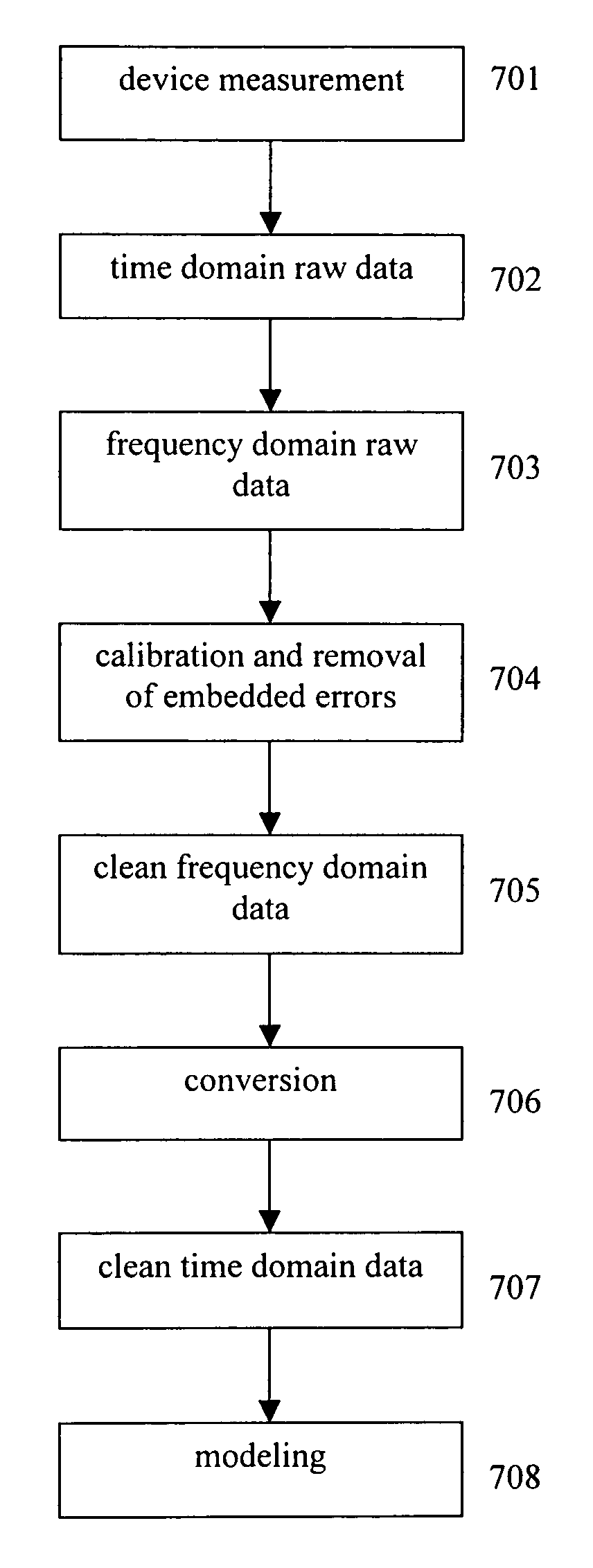
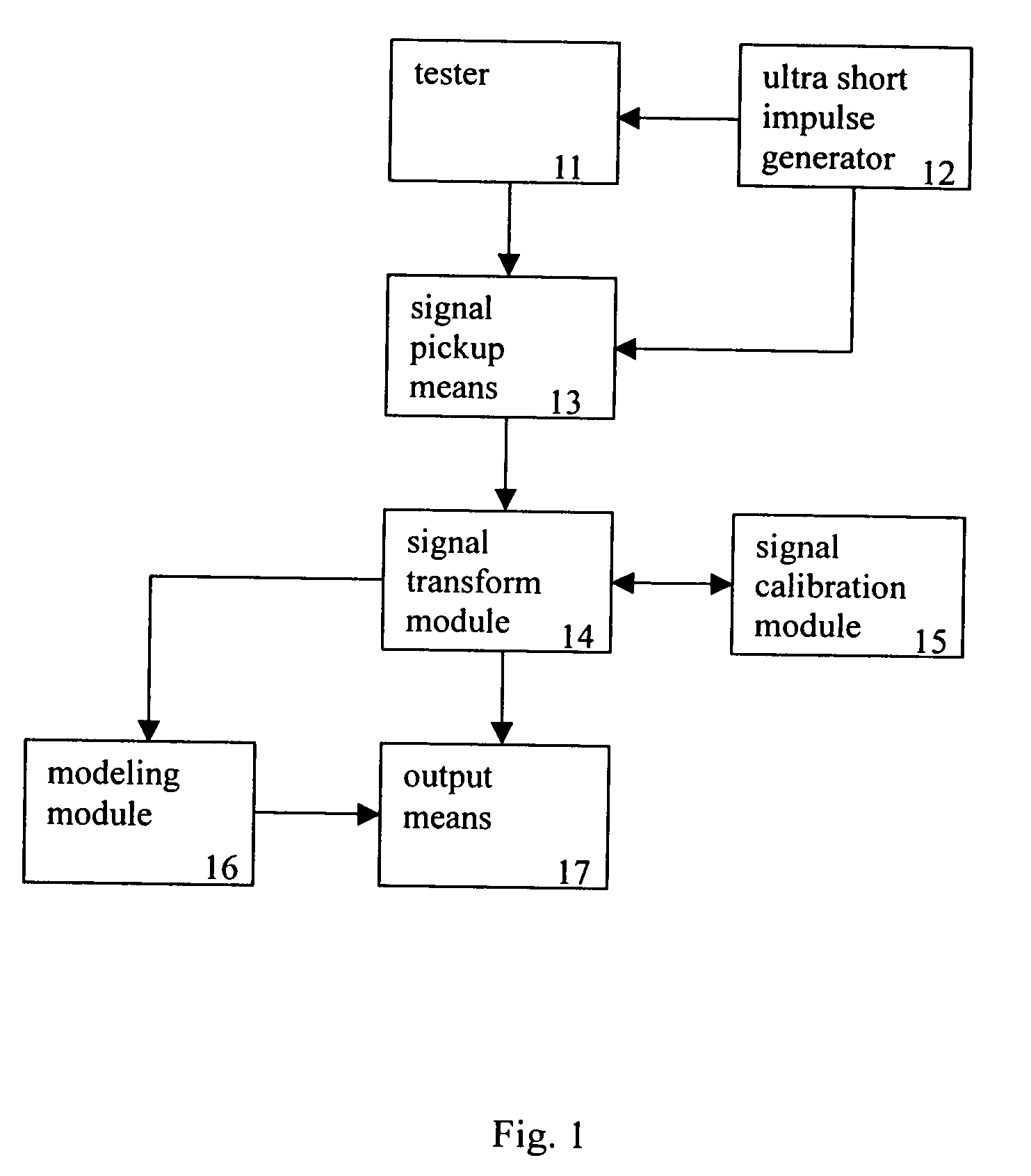
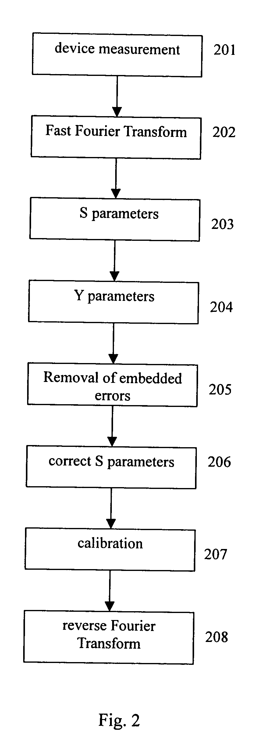
[0020]Although it is not intended to limit the scope of this invention, it is found that, if the equivalent model of an electronic device is able to faithfully describe an ultra short time domain response, the model shall conform the requirements in the wideband, nonlinear and ultra high-frequency considerations of the device. In the present invention, an ultra short impulse with duration of less than 100 ps is applied to the electronic device to be measured. The ultra short impulse itself and its reflection response and transmission response are measured. The data so obtained are time domain data and are then transformed into frequency domain data. Calibration and removal of embedded errors are conducted using the frequency domain data to obtain clean data representing characteristics of the device. According to this invention the reflection response and the transmission response obtained using the ultra short impulse contain descriptive information of the characteristics of the de...


PUM


Abstract

The method for wideband device measurement and modeling includes: measurement of an electronic device to obtain a set of time domain raw data representing characteristics of said device; conversion of said time domain raw data into frequency domain raw data; calibration and correction of embedded errors according to said frequency domain raw data to obtain clean frequency domain data representing characteristics of said device; conversion of said frequency domain data into time domain clean data; and establishment of equivalent model of said device according to said time domain data. The time domain raw data are obtained by applying to said device an ultra short impulse and measuring said impulse and its response from said device. Conversion between said time domain data and said frequency domain data may be Fourier transform.

Description

FIELD OF THE INVENTION[0001]The present invention relates to method and system for measurement and modeling of electronic devices, especially to method and system for measurement and modeling of the wideband characteristics of devices, and more specifically, to method and system for measurement and establishment of equivalent model of electronic devices using ultra short impulses.BACKGROUND OF THE INVENTION[0002]Correct modeling of electronic devices is deemed fundamental for integrated circuit (IC) design. The IC design flow starts with the device measurement and modeling. The modeling results are then used for analog, digital, or mixed signal circuit design. When the silicon measurement results are different from simulation results, designers would return to circuit design modification and simulation and initiate further fabrication of the IC. Incorrect models cannot assure proper design. Any unsuccessful iteration of the flow will bring about the increase of cost. Today's challen...

Claims


Application Information

Patent Timeline
Patent Type & Authority Patents(United States)
IPC IPC(8): G01R31/00
CPCG01R27/28
Inventor HSU, YUNG-JANECHIOU, MING-HSIANG
Owner FRONTEND ANALOG & DIGITAL TECH CORP
Why Eureka
Try Eureka