Method of fabricating n-type semiconductor diamond, and semiconductor diamond

a technology of semiconductor diamond and n-type, which is applied in the direction of crystal growth process, polycrystalline material growth, chemically reactive gas growth, etc., can solve the problems of preventing the obtaining of desired device properties, insufficient method, and insufficient large-area film or crystallinity growth, etc., to achieve high doping efficiency, high quality, and high carrier density

Inactive Publication Date: 2007-02-06
SUMITOMO ELECTRIC IND LTD
View PDF10 Cites 12 Cited by
  • Summary
  • Abstract
  • Description
  • Claims
  • Application Information

AI Technical Summary

Benefits of technology

[0008]Recently, in view of the use of diamond as a semiconductor device such as a UV light emitting element or the like, both a high quality and a large surface area are required of a single-crystalline substrate available for epitaxial growth.

Problems solved by technology

However, there have been problems that there can be obtained no single-crystalline {111} diamond substrate of high quality and having a large surface area, even using a method of high-pressure synthesis or a method of vapor-phase synthesis.
However, this method is also, in view of application to semiconductor devices, insufficient in terms of the growth of large-area films or the crystallinity.
However, while this method can be expected to reduce cost and provide a large surface area, adverse influences due to crystal grain boundaries will prevent from obtaining desired device properties.
However, one problem in this regard is that the n-doping efficiency of an epitaxial layer would be extremely low, and no effective carrier density could be obtained as an electrically conductive diamond, if diamond would be caused to epitaxially grow while doping the single-crystalline {100} diamond substrate.

Method used


Image

  • Method of fabricating n-type semiconductor diamond, and semiconductor diamond
  • Method of fabricating n-type semiconductor diamond, and semiconductor diamond
  • Method of fabricating n-type semiconductor diamond, and semiconductor diamond

Examples


example 1

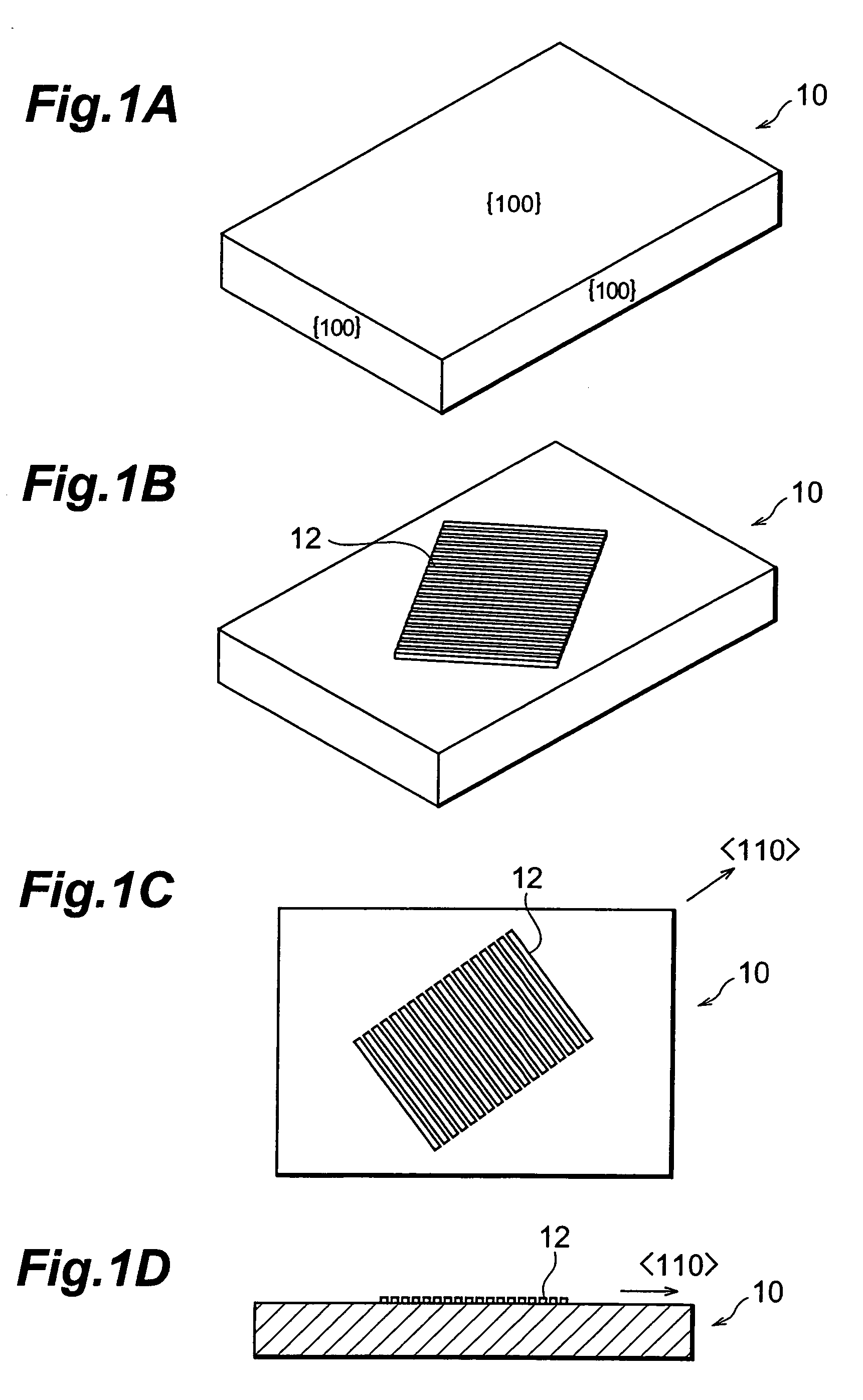
[0108]There was prepared a single crystal {100} diamond substrate which was cut such that the orientations of the top surface and side faces are {100} as shown in FIG. 1A. As shown in FIG. 1B, there was formed by a photo-lithography method, in the direction on a part of the surface of the single-crystalline {100} diamond substrate, an Al thin film mask 12 (film thickness of 0.5 μm) having a line and space pattern with the line width of 5 μm and the pitch of 5 μm.

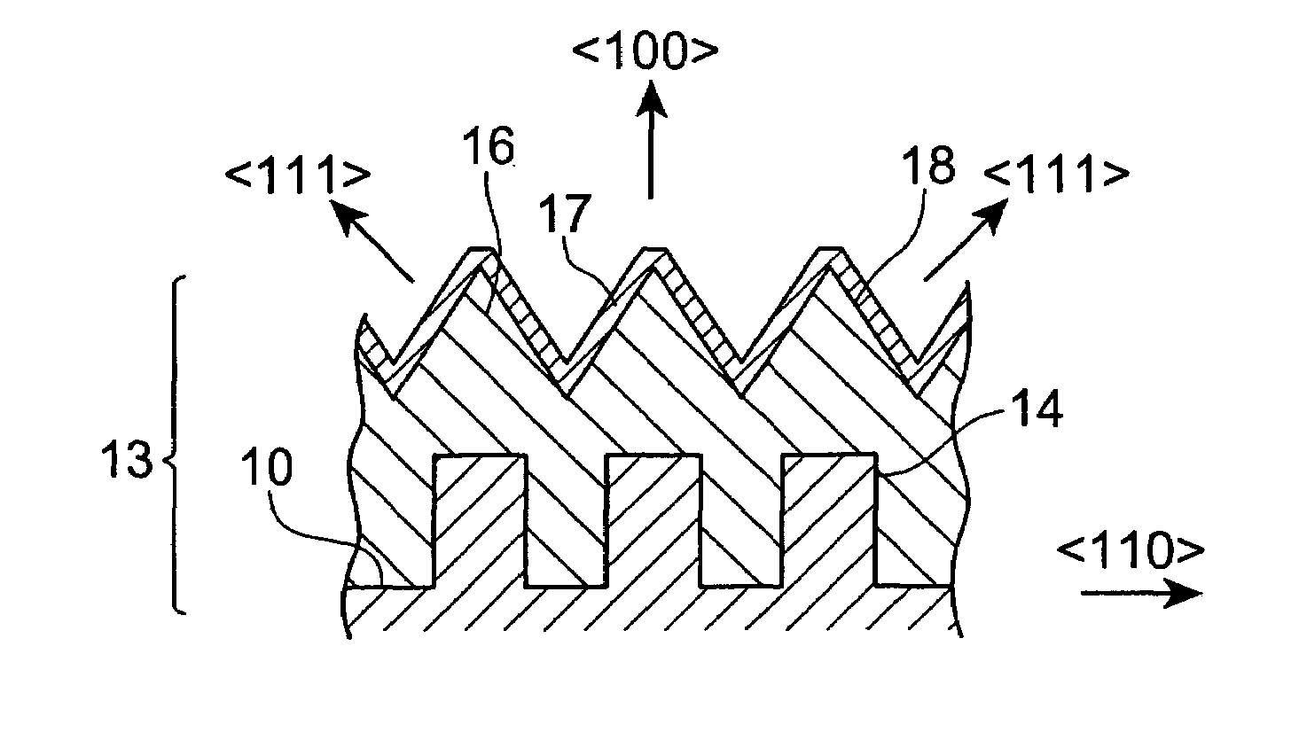
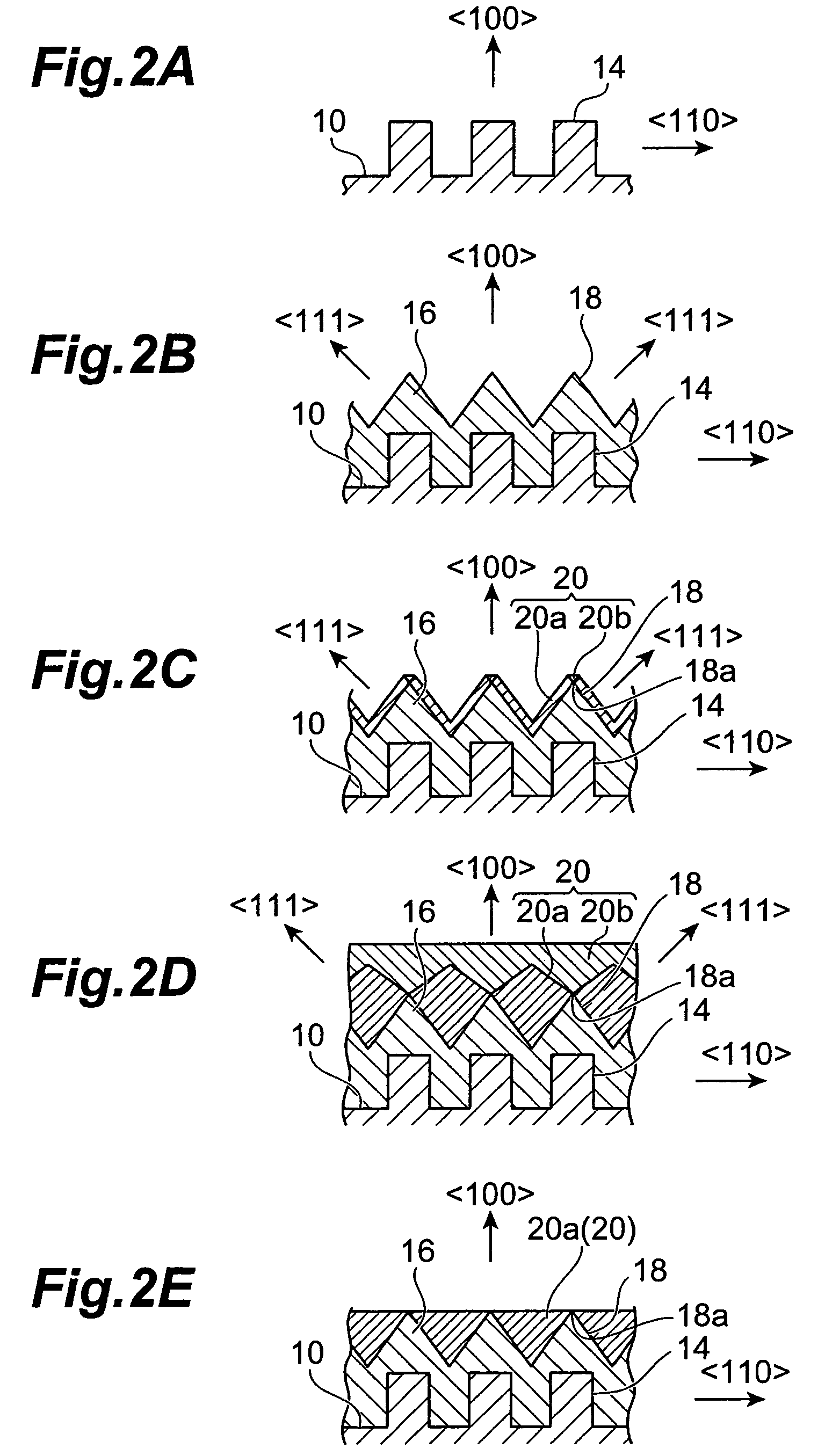
[0109]Next, The single-crystalline {100} diamond substrate patterned with the Al thin film mask 12 was transferred to dry etching device, and subjected to reactive ion etching under the conditions as follows: 99% O2 and 1% CF4 as etching gas; 200 W RF power; pressure of 6.6 Pa; 40 minutes of etching time; and 7 μm of etching depth. After that, Al thin film mask 12 was removed by means of Semico Clean. This causes, as shown in FIG. 2A, the diamond rectangular protrusion 14, rectangular in shape of a cross section and extendi...

example 2

[0119]As is the case with the first example, there was prepared a single-crystalline {100} diamond substrate 10 which was cut such that the orientations of the upper face and side faces were {100}. Next, as shown in FIG. 3B, by means of photolithography, on the surface of the single-crystalline {100} diamond substrate 10 there were formed in a matrix form a plurality of circular Al thin film masks 12 with a 5 μm diameter and a 10 μm center distance.

[0120]Next, the single-crystalline {100} diamond substrate 10 patterned with the Al thin film mask 12 was transferred to dry etching device, and was subjected to restrictive ion etching under the condition similar to that of the first example. After that, Al thin mask 12 was removed using Semico Clean. This caused, as shown in FIG. 3C, a plurality of cylindrical protrusions 22 made of cylindrical diamond, arrayed side-by-side in a matrix form, to be formed on the single-crystalline {100} diamond substrate 10.

[0121]Then, using microwave pl...

example 3

[0129]As is the case with the first example, photolithography and reactive ion etching were applied to the single-crystalline {100} diamond substrate 10. This allowed the rectangular protrusion 14 extending in one direction of to be formed on the surface layer of the single-crystalline {100} diamond substrate 10. In FIG. 13A there is shown this rectangular protrusion 14 in a cross section taken along the plane perpendicular to the extension direction thereof. The cross section of this rectangular protrusion 14 is of the size of 5 μm width and 7 μm height. Further, the distance between adjacent rectangular protrusions 14 is 5 μm.

[0130]Next, using microwave plasma CVD device, the non-doped diamond layer 16 was formed on the rectangular protrusion 14. On this occasion the synthesis condition for the non-doped diamond is set as follows: hydrogen gas flow rate of 0.11 / min (100 sccm); methane gas flow rate of 5×10⁻³ l / min (5 sccm); pressure of 1.3×10⁴ Pa; microwave power of 300 W; substr...


PUM

PropertyMeasurementUnit
angleaaaaaaaaaa
band gapaaaaaaaaaa
distanceaaaaaaaaaa

Abstract

An n-type diamond epitaxial layer 20 is formed by processing a single-crystalline {100} diamond substrate 10 so as to form a {111} plane, and subsequently by causing diamond to epitaxially grow while n-doping the diamond {111} plane. Further, a combination of the n-type semiconductor diamond, p-type semiconductor diamond, and non-doped diamond, obtained in the above-described way, as well as the use of p-type single-crystalline {100} diamond substrate allow for a pn junction type, a pnp junction type, an npn junction type and a pin junction type semiconductor diamond to be obtained.

Description

[0001]This application of CON of PCT / JP03 / 07717 filed Jun. 18, 2003.FIELD OF THE INVENTION[0002]The present invention relates to a method of fabricating n-type semiconductor diamond; to an n-type semiconductor diamond; to a pn junction type semiconductor diamond; to a pnp junction type semiconductor diamond; an npn junction type semiconductor diamond; and to a pin junction type semiconductor diamond.BACKGROUND OF THE INVENTION[0003]Great efforts in studies and researches are currently being made to be able to apply a diamond to usages as semiconductor device materials. Semiconductor devices employing diamonds can stably operate even in harsh environments of a high temperature, a space or the like, and can also cope with high-speed high-output operations, resulting in increasing demand.[0004]The applicability of diamonds as semiconductor device materials requires a conductivity type control pertaining to p-type or n-type. P-type semiconductor diamond can be easily obtained for exampl...

Claims


Application Information

Patent Timeline
Patent Type & Authority Patents(United States)
IPC IPC(8): H01L21/44C30B25/02C30B29/04H01L21/04H01L21/20H01L21/205
CPCC30B25/02C30B29/04H01L29/66037H01L21/02376H01L21/0243H01L21/02433H01L21/02444H01L21/02494H01L21/02527H01L21/02576H01L21/02587H01L21/02609H01L21/0262H01L21/02658H01L21/041H01L29/66022H01L21/20H01L21/205H01L27/12
Inventor NAMBA, AKIHIKOIMAI, TAKAHIRONISHIBAYASHI, YOSHIKI
Owner SUMITOMO ELECTRIC IND LTD
Why Eureka
Try Eureka