Arranging a plurality of imaging pixels in an imaging acquisition apparatus

a technology of imaging acquisition apparatus and plurality of imaging pixels, which is applied in the direction of color signal processing circuits, instruments, television systems, etc., can solve the problems of limited signal processing capacity, difficult to realize, and limited format conversion processing of signals in such processes, so as to improve the degree of freedom in design

Inactive Publication Date: 2007-02-06
OLYMPUS CORP
View PDF17 Cites 46 Cited by
  • Summary
  • Abstract
  • Description
  • Claims
  • Application Information

AI Technical Summary

Benefits of technology

[0013]Accordingly, an object of the present invention is to provide an image acquisition apparatus which, by totally relating an imaging optical system, an imaging element arrangement and a restoration processing, improves the degrees of freedom in design of an imaging section under strict constraints.

Problems solved by technology

However, the signal processing in such processes is limited to format conversion processing or inter-polation processing, or to color conversion processing, edge enhancing processing or the like for improving the appearance.
Further, in a case where the capacity of the signal is limited because the transfer band of the image signal is narrow, when a conventional digital image data compression method must be employed, an image structure of a sufficiently large scale is required regardless of the imaging elements, and further, a processor which realizes digital compressing functions must be loaded at the imaging section.
With such a system, it is extremely difficult to realize, for example, a system monitoring detailed functions in industrial facilities, visual functions of microrobots, extremely minute endoscopes used in medical diagnosis, or the like.
Moreover, because the image restoration processing is simple interpolation processing, it is only applicable to cases where the imaging pixels are arranged uniformly and systematically.
Namely, no method has been proposed which, even when, due to some constraint, only a lens having inferior performances can be loaded and the spatial frequency transfer characteristics differ greatly due to the position within the imaging surface, is suited for such conditions, and also can carry out efficient imaging by arranging pixels irregularly.
In addition, there has been no clear disclosure of an interpolation method suited for irregular pixel arrangements.
In this way, there has not been proposed a method which improves the degrees of freedom in design of the imaging section under strict constraints, by completely correlating the imaging optical system and the imaging pixel arrangement and the restoration processing in a conventional imaging / display system using solid-state imaging elements.

Method used


Image

  • Arranging a plurality of imaging pixels in an imaging acquisition apparatus
  • Arranging a plurality of imaging pixels in an imaging acquisition apparatus
  • Arranging a plurality of imaging pixels in an imaging acquisition apparatus

Examples


first embodiment

(First Embodiment)

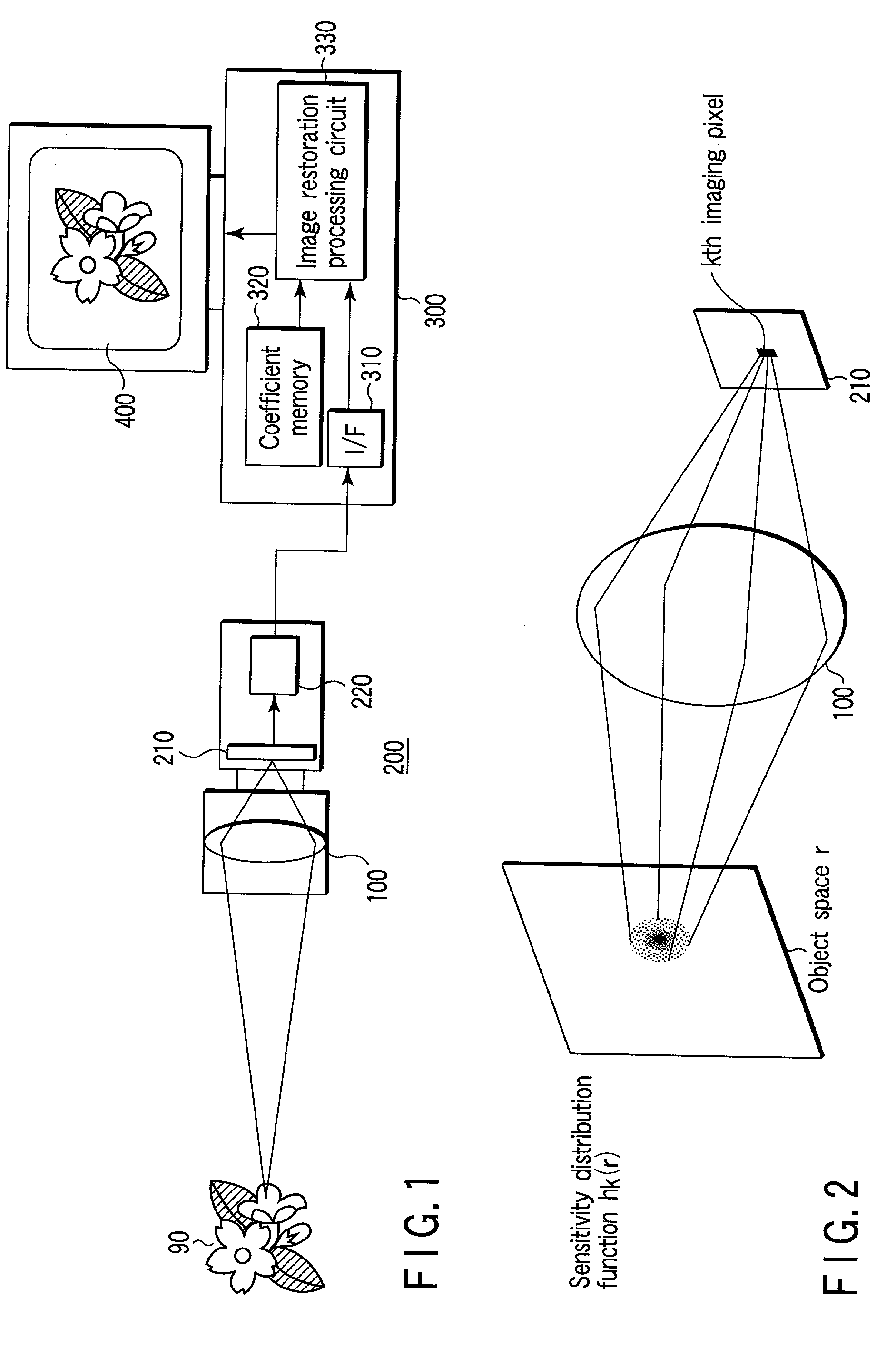
[0037]FIG. 1 is an overall structural view of an image acquisition apparatus according to a first embodiment of the present invention. The image acquisition apparatus is structured from a lens 100 as an imaging optical system, an imaging section 200, an image restoration processor 300 as an image restoration processing section, and a monitor 400.

[0038]An image of an object 90 imaged by the lens 100 is photoelectrically converted by an imaging element 210 in the imaging section 200, and is converted to an appropriate image signal in an image signal output circuit 220, and is outputted.

[0039]At the image restoration processor 300, the image signal from the imaging section 200 is inputted via an interface (I / F) 310, and is transferred to an image restoration processing circuit 330. Note that, when the sent image signal is an analog signal, the signal is converted to an appropriate digital signal in the I / F 310. On the other hand, coefficients suiting the conditions of...

second embodiment

(Second Embodiment)

[0115]A second embodiment of the present invention is a modified example of the imaging pixel arrangement in the imaging element. FIG. 8 shows a structural example of the second embodiment. Imaging pixels are disposed randomly throughout an entire imaging surface of a CMOS imaging element 213. Here, the definition of random is that the following two conditions are satisfied simultaneously.

[0116](i) There is no regularity to the distribution of the intervals between adjacent pixels.

[0117](ii) The existence concentration within a local region having a predetermined surface area is uniform and does not depend on the position of that local region.

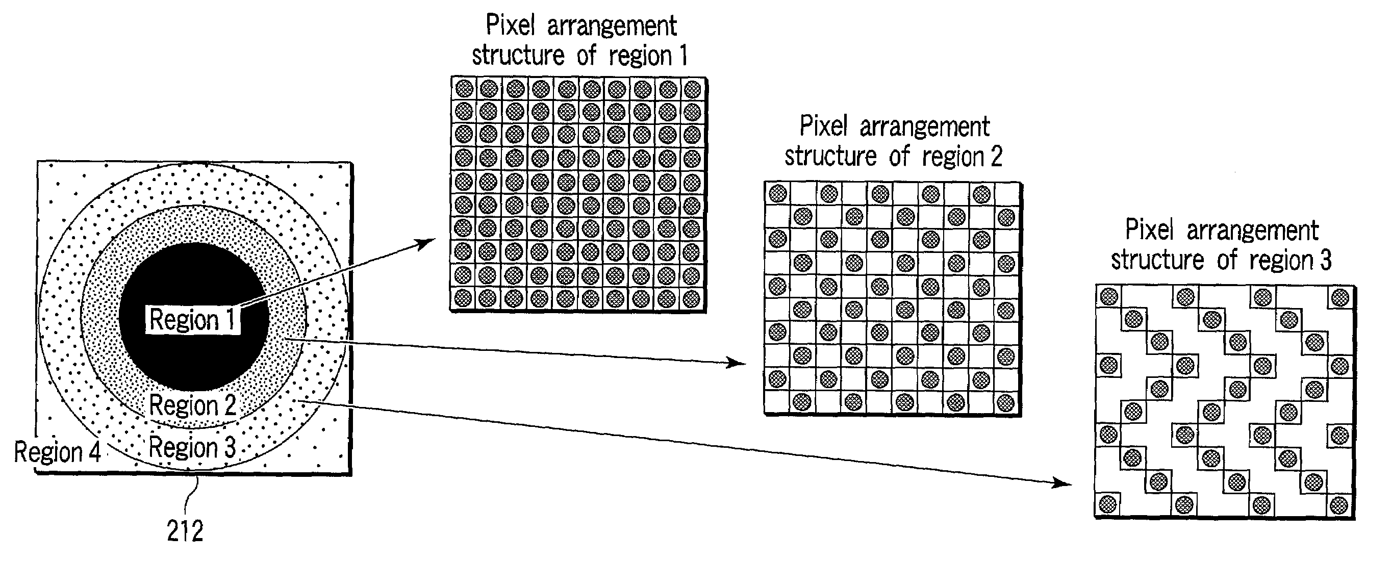
[0118]FIG. 9 shows another structural example. The imaging surface of the imaging element is divided into four regions (region 1 through region 4) in a concentric circle form as shown in the left-hand drawing. In the same way as FIG. 6, for each region, the concentration of the pixels greatly differs. Within each region, the ...

third embodiment

(Third Embodiment)

[0122]The third embodiment of the present invention is an example in which imaging elements are structured by mosaic color type elements. FIG. 10 shows a structural example of the third embodiment. In the same way as FIG. 6 of the first embodiment, the imaging surface of a CMOS imaging element 215 is divided into four regions (region 1 through region 4) in a concentric circle form, and in accordance with moving from the center toward the periphery of the imaging surface, the concentration of disposed pixels becomes smaller region-by-region. Further, the pixel arrangement in each region is realized by systematic thinning. In this pixel arrangement structure, in order to realize a color imaging element, the arrangement of color filters mounted to the light receiving surface of each imaging pixel is random. Namely, when a method is used in which a color image is picked up by filters of the three primary colors of red (R), green (G), and blue (B), the arrangement for e...


PUM


Abstract

An image acquisition apparatus has an imaging optical system. An imaging section has a plurality of imaging pixels arranged at non-uniform intervals within an imaging surface. The imaging section picks up an object image imaged by the imaging optical system, and converts the object image into image signals. An image restoration processing section has a coefficient memory in which a predetermined coefficient sequence is recorded, and an image restoration processing circuit which carries out computation processing between the coefficient sequence recorded in the coefficient memory and the image signals from the imaging section. The image restoration processing section generates an image in a desired display pixel arrangement.

Description

CROSS-REFERENCE TO RELATED APPLICATIONS[0001]This application is based upon and claims the benefit of priority from the prior Japanese Patent Application No. 2001-088380, filed Mar. 26, 2001, the entire contents of which are incorporated herein by reference.BACKGROUND OF THE INVENTION[0002]1. Field of the Invention[0003]The present invention relates to an image acquisition apparatus.[0004]2. Description of the Related Art[0005]In the technical field of image acquisition, in a solid-state imaging element such as a CCD, generally, the respective imaging pixels are arranged in a square lattice form. Further, the output image signal from a camera formed by using such imaging elements is converted into and used in an appropriate time-series signal format in accordance with the application. For example, if the camera is a camera for movies, the image signal is output by an analog video format such as NTSC or S-VHS or the like, and is displayed on a monitor. If the camera is a digital stil...

Claims


Application Information

Patent Timeline
Patent Type & Authority Patents(United States)
IPC IPC(8): H04N5/335G06K9/32G09G5/02H04N7/18H04N9/083H04N9/74G06T1/60H04N5/232H04N5/374H04N9/07
CPCH04N5/3696H04N5/335H04N25/00H04N25/702
Inventor KIKUCHI, SUSUMU
Owner OLYMPUS CORP
Why Eureka
Try Eureka