Device for and method of examining the signal performance of semiconductor circuits

Inactive Publication Date: 2007-02-13
POLARIS INNOVATIONS
View PDF4 Cites 1 Cited by
  • Summary
  • Abstract
  • Description
  • Claims
  • Application Information

AI Technical Summary

Benefits of technology

[0017]A further advantage of the present invention is that data on the distribution of the internal delay time and thus on the velocity of a plurality of integrated semiconductor circuits are automatically acquired, wherein these data can for example be evaluated statistically so that statements an process variations and their effects on the electric performance of the integrated semiconductor circuit produced can be made therefrom.
[0018]With the help of the data acquired the existing circuit simulation models can be refined, i.e. the velocity variations due to technical process variations can be predicted more precisely for the future and thus be better included in the circuit simulation.
[0019]A further advantage of the present invention is that an exact determination of any asynchronous signal is possible in a system which, due to the operating cycle, is fully synchronous under production conditions. This is required since the internal delay time of the semiconductor circuit to be determined is arbitrary, which means that it does not necessarily occur in a synchronous way relative to the operating cycle of the integrated semiconductor circuit.
[0020]A further advantage of the present invention is that the automatic determination of the internal delay time of integrated semiconductor circuits is also facilitated in the case of a parallel testing of a plurality of integrated semiconductor chips, since the data measured is filed in different regions of the error memory of the semiconductor tester and the data can be evaluated after completing the test, if several chips are simultaneously tested under production conditions.
[0021]According to a further aspect of the present invention a variation of the length of the input test pulse can additionally be detected by a circuit under test. Thus a input test signal is for example fed into the circuit under test, the input test signal having a test signal pulse with a predetermined length, this pulse for example being defined by a first rising an a second falling signal edge (or vice versa). The output signal is then sampled at the output of the circuit under test, this signal being a response to the test signal pulse of the input test signal.
[0022]The sampling occurs at predetermined times to obtain a sequence of sample values, wherein, as in the first embodiment, a first state is associated to a sample value when the output signal has a first signal value and a second state is associated to a sample value when the output signal has a second signal value. In the following the number of sample values to which an equal state is associated is counted, i.e. the sample values corresponding to the output signal pulse of the circuit under test are counted. With the help of this number of sample values the length of the output signal of the circuit under test can be determined knowing the respective time interval between the predetermined sampling times. The intervals between the predetermined sampling times can differ.

Problems solved by technology

With this modified circuit simulations, however, the velocity variations of the integrated semiconductor circuits, really occurring during the production of same, due to process variations naturally cannot be predicted exactly.
This manual examination, however, on the one hand requires lots of personnel and on the other hand, as expected, does not cover the entire process window, i.e. the predetermined velocity interval.
In addition the personnel required for the examination of the chip performance contributes considerably to the production cost of semiconductor circuits.

Method used


Image

  • Device for and method of examining the signal performance of semiconductor circuits
  • Device for and method of examining the signal performance of semiconductor circuits
  • Device for and method of examining the signal performance of semiconductor circuits

Examples


Embodiment Construction

[0030]In the following, the inventive concept for detecting a delay time of a circuit, especially of an integrated semiconductor circuit, is detailed to be able to automatically determine the velocity of logic circuits.

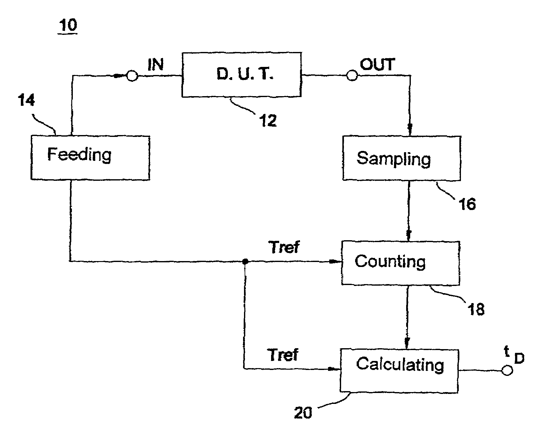
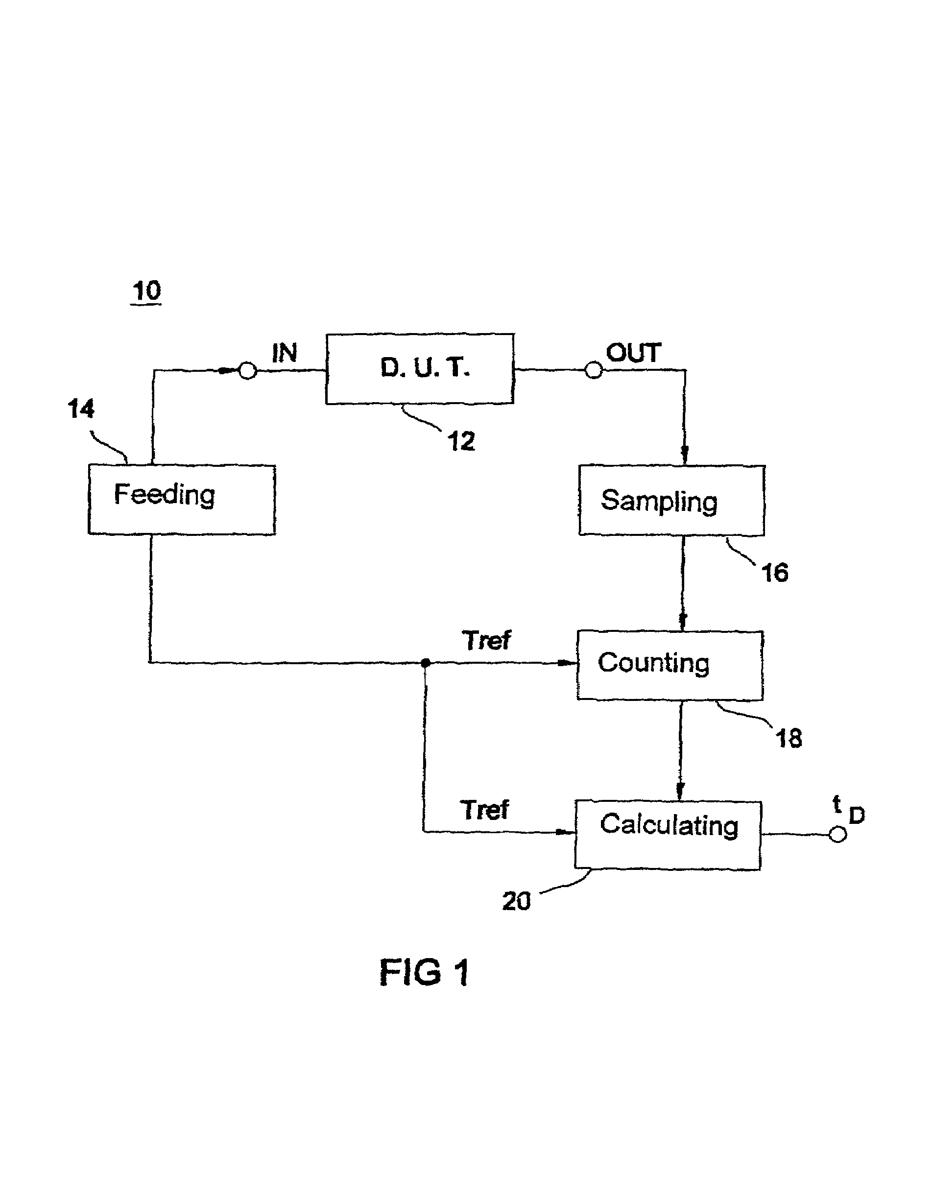
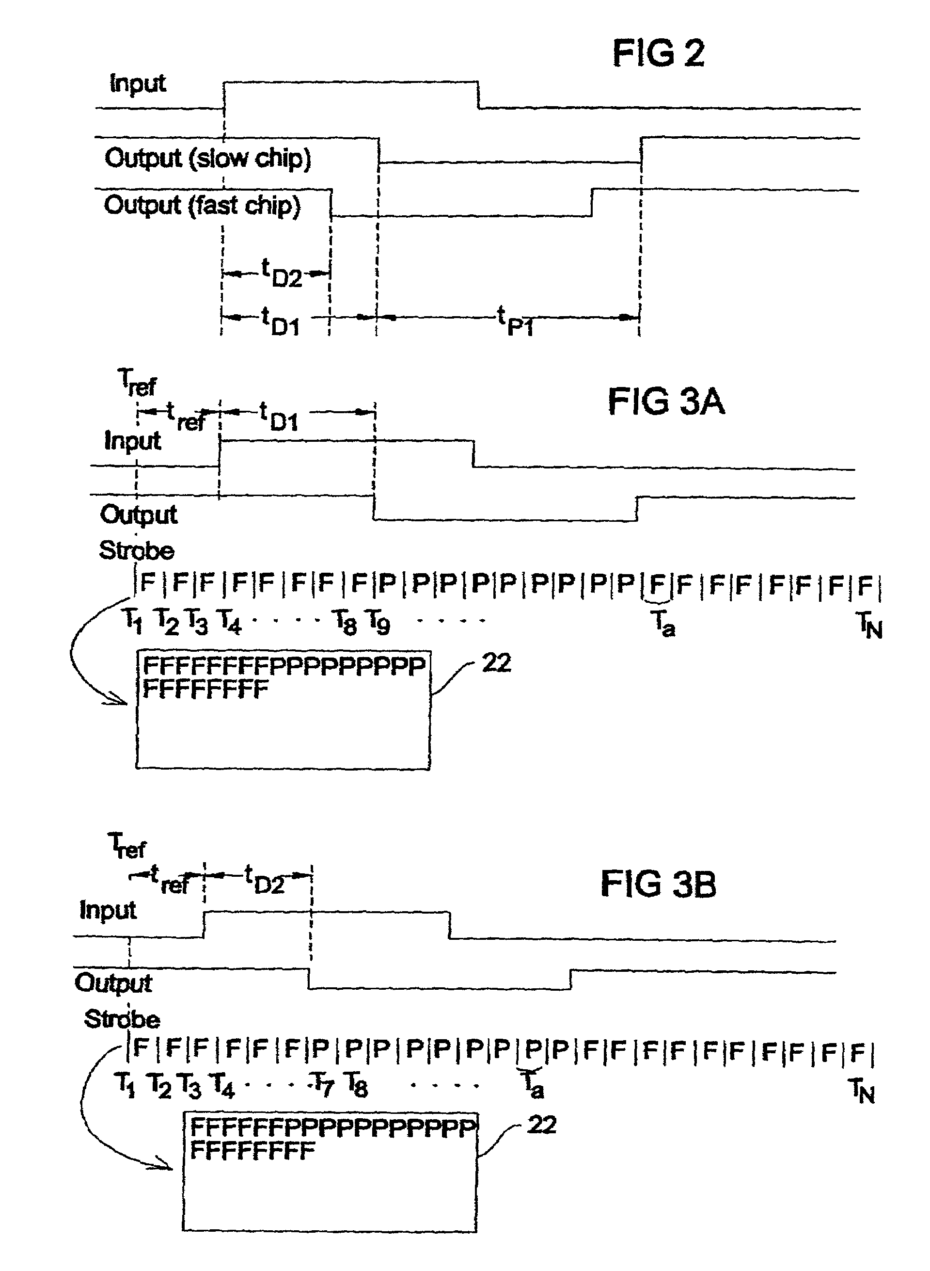
[0031]In FIG. 1 a device 10 for detecting a delay time tD of a circuit under test 12 (DUT; DUT=device under test) is illustrated in principle. Thus the delay time subsequently called tD1 represents the relatively long delay time of a slow chip, while the delay time subsequently called tD2 represents the relatively short delay time of a fast chip. The device 10 comprises feeding means 14 to feed a test signal into the circuit under test 12 at the input side. The circuit under test 12 is connected to sampling means 16 at the output side, this means sampling the output signal of the circuit under test 12 at predetermined times T1, T2, . . . TN to obtain a sequence of sample values therefrom. The output of sampling means 16, at which the sequence of sample values is provi...


PUM


Abstract

A device and method for detecting a delay time of a circuit is provided. A test signal is fed into the circuit, the test signal including a signal edge, the occurrence of which is related to a reference time. The output signal of the circuit is sampled at predetermined times to obtain a sequence of sample values, with a first state being associated with a sample value when the output signal has a first signal value and a second state being associated with a sample value when the output signal has a second signal value. A counter counts the sample values of the sequence, to which an equal state is associated, to obtain counted sample values. A delay time is calculated using the counted number of sample values.

Description

FIELD OF THE INVENTION[0001]The present invention relates to a device for and a method of detecting the delay times of semiconductor circuits and especially to the detection of the delay times of semiconductor circuits by means of a semiconductor tester.BACKGROUND OF THE INVENTION AND PRIOR ART[0002]In the field of integrated semiconductor circuits the ever-smaller minimal structural dimensions of the respective circuit elements pose ever-higher demands on the production processes of integrated semiconductor circuits. To the same extent the demands on the so-called chip performance also increase. For this reason it is tried to already take account of process variations unavoidable in practice, if possible, in the circuit simulation of the integrated semiconductor circuit. This results in interval regions for the chip performance, within which the chip performance should typically be. With this modified circuit simulations, however, the velocity variations of the integrated semicondu...

Claims


Application Information

Patent Timeline
IPC IPC(8): G11B20/20G01R31/28G01R31/3193
CPCG01R31/31937
Inventor KEIM, MARTINKUND, MICHAEL
Owner POLARIS INNOVATIONS
Why Eureka
Try Eureka