Optical cross-connect system

a cross-connect switch and optical technology, applied in the field of optical communication, can solve the problems of physical damage to the landing pad, loss of clamping voltage, loss of switch state,

Inactive Publication Date: 2007-02-27
ANALOG DEVICES INC
View PDF116 Cites 48 Cited by
  • Summary
  • Abstract
  • Description
  • Claims
  • Application Information

AI Technical Summary

Problems solved by technology

While the insulating landing pad material does, indeed, prevent an electrical short, its inherent properties can lead to other problems.
Firstly, most insulating materials have the capacity to trap electrical charge and can, in some cases, maintain that charge for long periods of time—sometimes indefinitely.
Such surges can lead to physical damage to the landing pads 122, 124 or the clamping surface, or may produce micro-welding, where the landing pad is welded to the clamping surface—resulting in the mirror 111 being stuck.
In the event of a power failure, the clamping voltage may be lost and any MEMS mirrors that were clamped in a specific state may revert to the opposing state when under the influence mechanical restoring forces.
In this manner, the state of the switch may be lost in the event of a power failure.
The increasing complexity of optical switching systems has lead to development of switching fabrics that are larger than say 8×8.
Unfortunately this is a lengthy development process.
Unfortunately, this complicates the overall design of the optical switch.
However, for 16×16 arrays and larger, the size of the array still presents problems even if smaller devices are tiled together.
The increased optical path between the fibers can lead to undesirable beam spreading.
However, the alignment of the collimator lenses to the switching elements is difficult and even slight misalignment will result in optical loss that degrades switch performance.
Another problem with tiling two or more dies is that the dies must be very accurately aligned with each other in order to ensure that the mirrors on one die will align with those on the other dies in the mosaic.
However, even using these techniques, alignment can be particularly problematic with a tiled device having four 8×8 MEMS mirror arrays totaling 256 MEMS mirrors.

Method used


Image

  • Optical cross-connect system
  • Optical cross-connect system
  • Optical cross-connect system

Examples


first embodiment

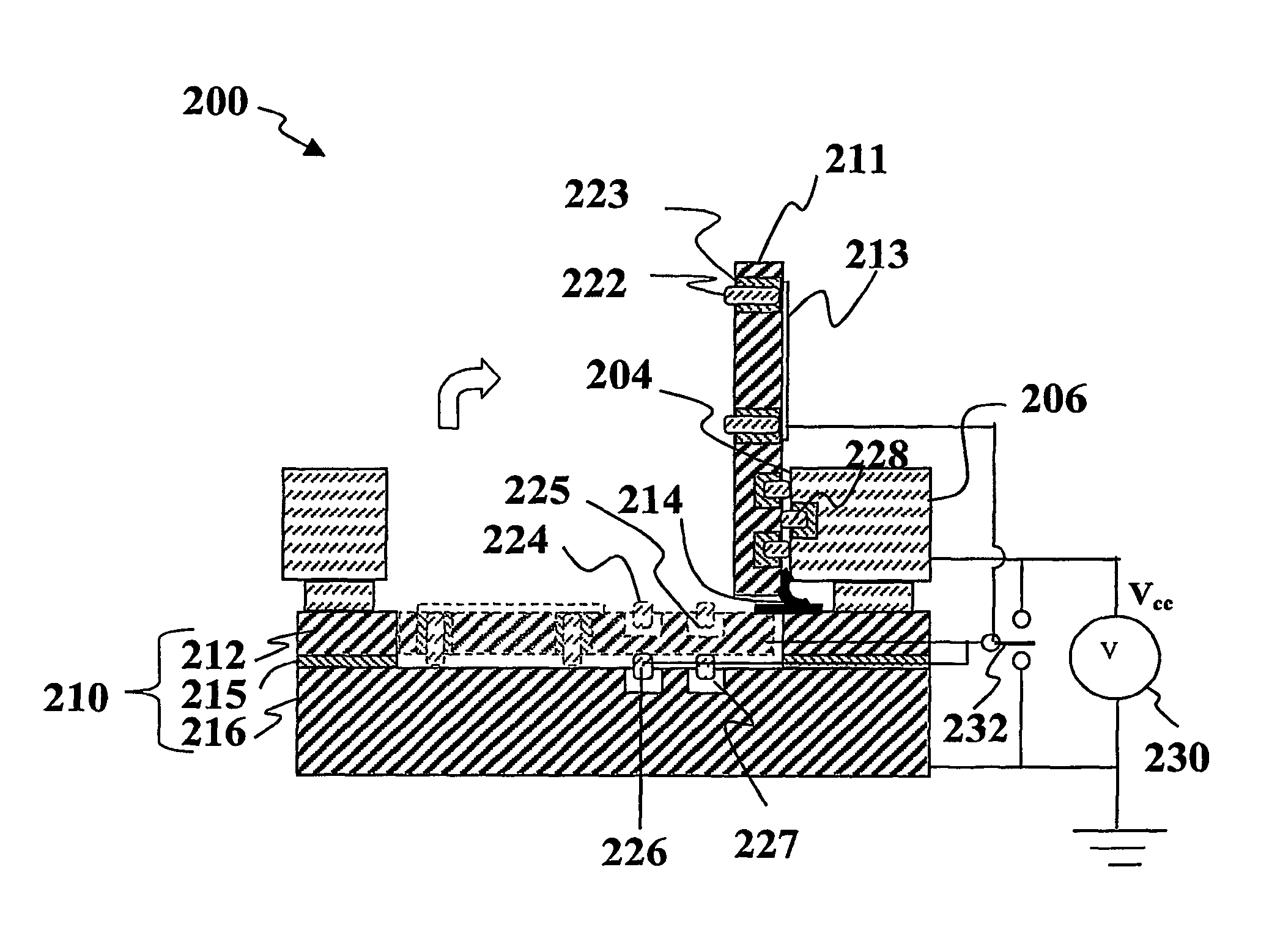
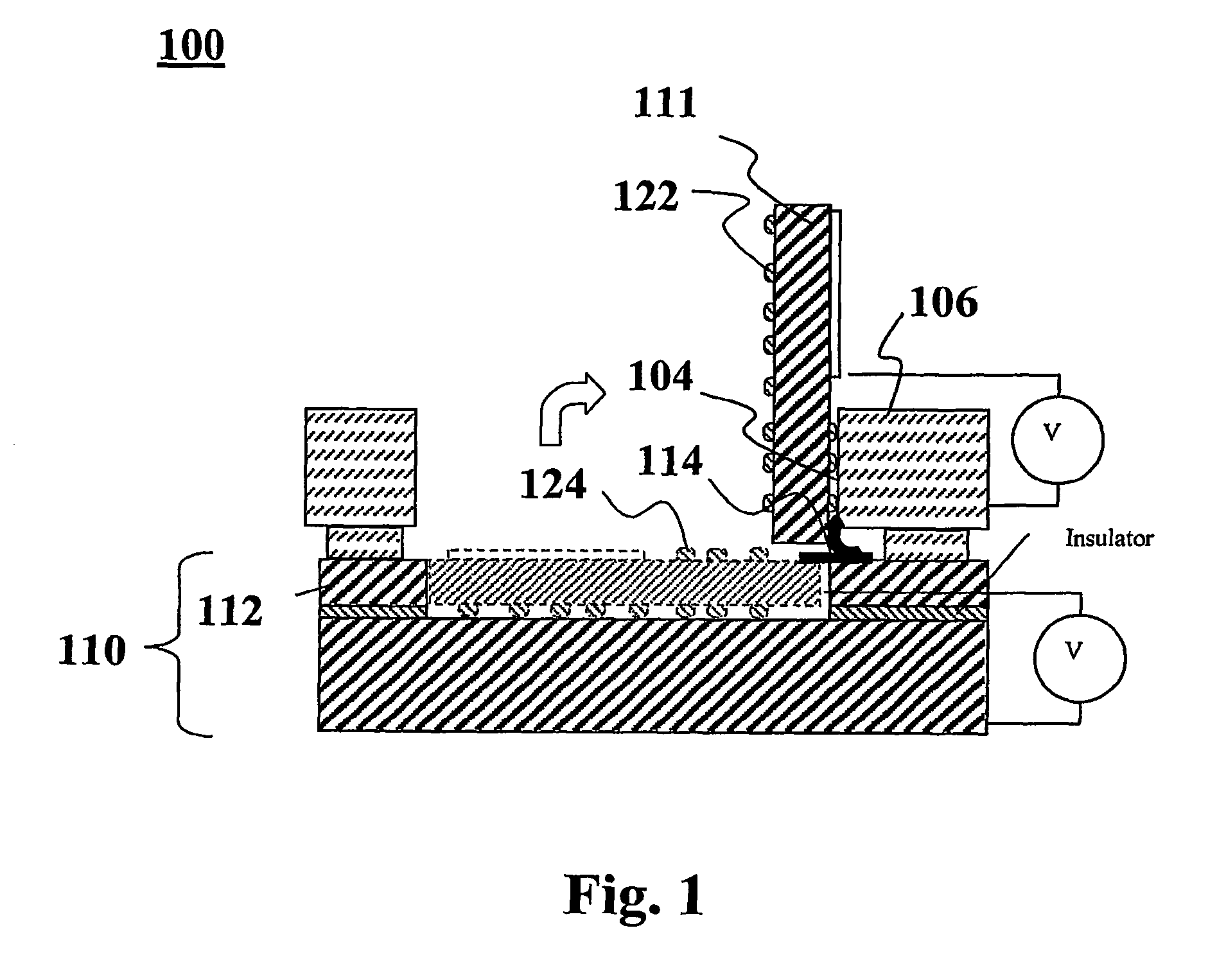
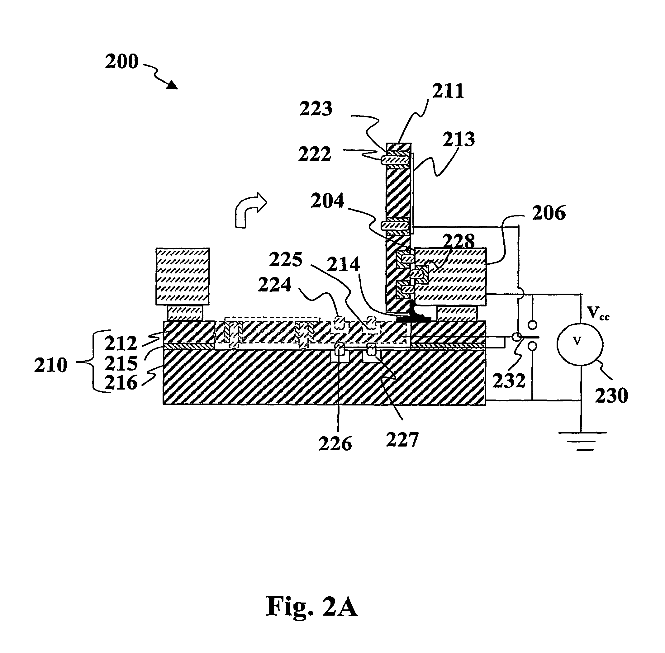
[0168]FIG. 17A depicts an exploded isometric diagram of a MEMS device 1700 according to the present invention. An assembly diagram of the device 1700 is depicted in FIG. 17B. The device 1700 may be used, for example, as an optical switch, as shown in FIG. 17B. The device 1700 may selectively couple optical signals 1701 between a first set of optical input / output (I / O) ports 1752 and a second set of I / O ports 1754 as shown in FIG. 17B. The I / O ports 1752, 1754 may be collimator lenses, such as graded refractive index (GRIN) lenses that couple the optical signals 1701 to and from optical fibers (not shown). To facilitate optical coupling to the I / O ports 1752, 1754, the device 1700 may include collimator arrays 1756 that are disposed along the perimeter of the device 1700. The device 1700 generally includes a substrate 1710, MEMS device dies 1720A, 1720B, 1720C, 1720D, and a common clamping die 1730. Each MEMS device die 1720A, 1720B, 1720C, 1720D may have an array of MEMS optical ele...

second embodiment

[0178]MEMS devices of the type shown in FIGS. 17A–17B may be manufactured according to an inventive method 1800 according to the invention. The steps of the method 1800 are illustrated in the flow diagram of FIG. 18. For the purposes of example, the steps of the method 1800 are described below with respect to the device 1700 of FIGS. 17A–17B. The method begins with the fabrication of MEMS device dies 1720A, 1720B, 1720C, 1720D by standard semiconductor processes. At an optional step 1802, the device dies may be tested prior to further assembly to ensure proper operation.

[0179]At step 1804, the device dies are attached to the substrate 1710. By way of example, the device dies 1720A, 1720B, 1720C, 1720D may be attached with a solder attachment process. For example, the metallized bonding pads 1716, 1726 react with a solder to form strong self-aligned bonds. The bonding pads 1716 on the substrate 1710 are preferably defined with the highest resolution processes available (e.g., thin fi...


PUM


Abstract

An optical cross-connect switch comprises a base (216), a flap (211) and one or more electrically conductive landing pads (222) connected to the flap (211). The flap (211) has a bottom portion that is movably coupled to the base (216) such that the flap (211) is movable with respect to a plane of the base (216) from a first orientation to a second orientation. The one or more landing pads (222) are electrically isolated from the flap (211) and electrically coupled to be equipotential with a landing surface.

Description

[0001]This application is a 371 of PCT / US02 / 09038, filed Mar. 1, 2002, which was a CIP of U.S. application Ser. No. 09 / 798,129, filed Mar. 1, 2001, now U.S. Pat. No. 6,528,887, which was a CIP of Ser. No. 09 / 851,587, filed May 8, 2001, now U.S. Pat. No. 6,906,511, which was a CIP of Ser. No. 09 / 853,868, filed May 11, 2001, which was abandoned, which was a CIP of Ser. No. 09 / 853,869, filed May 11, 2001, which was abandoned, which was a CIP of Ser. No. 09 / 853,870, filed May 11, 2001, now U.S. Pat. No. 6,891,988, which was a CIP of Ser. No. 09 / 891,760, filed Jun. 25, 2001, now U.S. Pat. No. 6,859,577, which was claims benefit of Ser. No. 60 / 303,755, filed Jul. 7, 2001, which was a CIP of 09 / 900,841, filed Jul. 7, 2001, now U.S. Pat. No. 6,514,781, which was a CIP of Ser. No. 09 / 949,210, filed Sep. 7, 2001, now U.S. Pat. No. 6,873,756, which was a CIP of Ser. No. 09 / 992,530, filed Nov. 6, 2001, which was abandoned, which was a CIP of Ser. No. 09 / 992,531, filed Nov. 6, 2001, which was ab...

Claims


Application Information

Patent Timeline
Patent Type & Authority Patents(United States)
IPC IPC(8): H01L23/02G02B26/08G02B6/42
CPCG02B6/3518G02B26/0841G02B6/3546G02B6/356G02B6/3572G02B6/3584G02B6/357
Inventor DANEMAN, MICHAEL J.WALL, FRANKLINBEHIN, BEHRANGCHAPARALA, MURALICHANG, MARK W.DALTON, SCOTTBEERLING, TIMOTHYPANYKO, STEPHENKIANG, MENG-HSIUNGKOBRIN, BORISLIN, CHUANG-CHIA
Owner ANALOG DEVICES INC
Why Eureka
Try Eureka