Method for operating a memory device

a memory device and nonvolatile memory technology, applied in the direction of read-only memories, instruments, static storage, etc., can solve the problems of nrom arrays posing a problem for mass storage or code flash applications, preventing fast parallel programming rates,

Inactive Publication Date: 2007-03-13
SPANSION ISRAEL
View PDF147 Cites 16 Cited by
  • Summary
  • Abstract
  • Description
  • Claims
  • Application Information

AI Technical Summary

Benefits of technology

[0029]Further in accordance with an embodiment of the invention the control circuit is adapted to adjust the duration of said the operation pulse.
[0030]Further in accordance with an embodiment of the invention the control circuit is adapted to adjust the amplitude of said second operation pulse.
[0027]In accordance with another embodiment of the invention a system for operating a set of memory cells in a memory array is provided. The system includes a memory array, a sense amplifier adapted to determine a response of operated cells, and a control circuit adapted to produce a first operating pulse to a terminal of a first cell intended to place the first cell into a predefined state. The control circuit is further adapted to determine pulse characteristics of a second operating pulse as a function of the response of the first cell to the first operating pulse.

Problems solved by technology

The application of pulses to operate (program or erase) the NROM array may pose a problem for mass storage or code flash applications.
Other complications that may hinder achieving fast, parallel programming rates include, among others, temperature dependence, cell length dependence (e.g., die to die and within a die), neighboring cell state dependence, second bit state dependence, and others.
Determination of programming pulses is also complicated by the fact that the cell parameters and operating conditions are usually initially unknown.
However, this may be disadvantageous because it may result in a wide and varied distribution of threshold voltages in the programmed cells of the array, which may reduce product reliability.
However, such a method may incur a substantial overhead in the form of multiple verify pulses (e.g., one per reference), which is an undesirable time penalty, or may require an intricate parallel reference design, which is an undesirable chip area penalty.

Method used


Image

  • Method for operating a memory device
  • Method for operating a memory device
  • Method for operating a memory device

Examples


Embodiment Construction

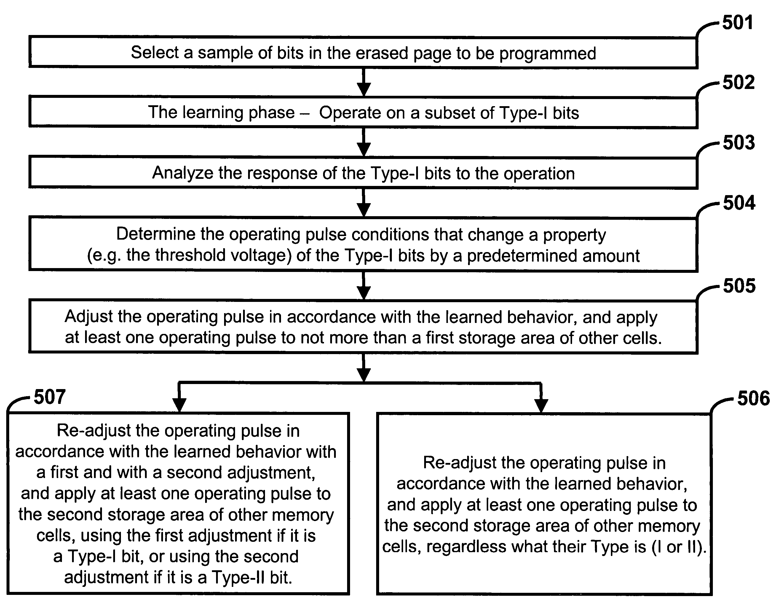
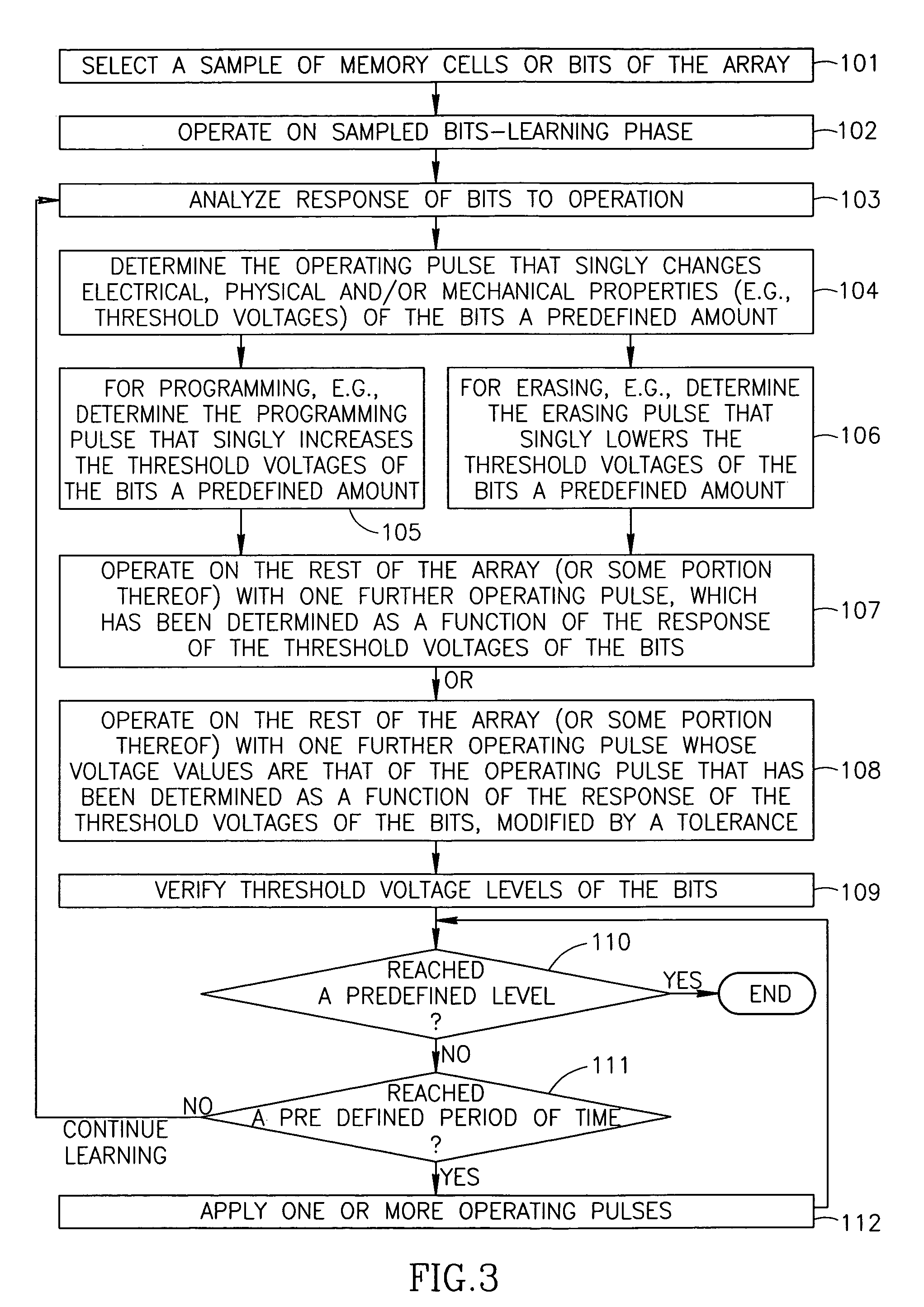
[0041]Reference is now made to FIG. 3, which illustrates a method for operating bits of memory cells in a memory cell array, in accordance with an embodiment of the present invention. FIG. 3 is shown and described herein for programming the bits, but it is appreciated that the invention is not limited to the operation of programming, and the invention may be applied to other operations, such as but not limited to, erasing.

[0042]A set of memory cells or bits of the array may be selected (step 101). The set size may be any arbitrary size, such as but not limited to, 64 cells, for example. The bits in the set may then be programmed (step 102), such as by using a stepped programming algorithm. A suitable stepped programming algorithm is the one described in the Applicant's abovementioned copending U.S. patent application Ser. No. 09 / 730,586, entitled “Programming And Erasing Methods For An NROM Array”. The method comprises applying progressive pulses or steps of programming voltages tha...


PUM


Abstract

A method and a system for operating bits of memory cells in a memory array, the method including applying a first operating pulse to a terminal of a first cell, the first operating pulse is intended to place the first cell into a predefined state; and applying a second operating pulse to a terminal of a second cell in the set, the second operating pulse is intended to place the second cell to the predefined state, and the pulse characteristics of the second operating pulse are a function of the response of the first cell to the first operating pulse.

Description

CROSS-REFERENCE TO RELATED APPLICATIONS[0001]The present application is a continuation-in-part application of U.S. Ser. No. 10 / 747,217, filed Dec. 30, 2003, which is a continuation-in-part application of U.S. Ser. No. 10 / 211,248, filed Aug. 5, 2002, issued as U.S. Pat. No. 6,700,818 on Mar. 2, 2004, which claims priority from U.S. provisional application Ser. No. 60 / 352,549, filed Jan. 31, 2002, both applications are hereby incorporated by reference in their entirety.FIELD OF THE INVENTION[0002]The present invention relates generally to operating memory cells of non-volatile memory (NVM) arrays, such as programming and erasing, and particularly to methods for reducing pulse operations of such arrays.BACKGROUND OF THE INVENTION[0003]Memory cells are used in the implementation of many types of electronic devices and integrated circuits, such as, but not limited to, erasable, programmable read only memories (EPROMs), electrically erasable, programmable read only memories (EEPROMs), and...

Claims


Application Information

Patent Timeline
Patent Type & Authority Patents(United States)
IPC IPC(8): G11C16/04G11C16/34G11C29/02G11C29/50
CPCG11C16/0475G11C16/10G11C16/3445G11C29/50004G11C29/02G11C29/021G11C29/028G11C29/50G11C16/3459G11C16/04G11C16/3436
Inventor MAAYAN, EDUARDOEITAN, BOAZ
Owner SPANSION ISRAEL
Why Eureka
Try Eureka