Method for removing post-etch residue from wafer surface

a post-etch residue and wafer surface technology, applied in the direction of basic electric elements, electrical equipment, semiconductor devices, etc., can solve the problems of complex composition of trench/via residuals, which are produced, and the prior art methods have been proved to be unsatisfactory, so as to achieve the effect of effectively removing post-etch residues

Active Publication Date: 2007-03-20
UNITED MICROELECTRONICS CORP
View PDF18 Cites 18 Cited by
  • Summary
  • Abstract
  • Description
  • Claims
  • Application Information

AI Technical Summary

Benefits of technology

[0011]It is the primary object of the present invention to provide an improved method for effectively removing post-etch residues in a trench / via opening.
[0012]It is another object of the present invention to provide a method for effectively removing post-etch residues in a trench / via opening, which is etched into low-k dielectric films with at least one metal layer as a hard mask.

Problems solved by technology

As pitches between interconnection wirings of integrated circuits shrink to very deep sub-micron scale or beyond, post-etch trench / via residual looms as a major issue regarding the success in damascene or dual damascene processes.
However, the results presented by the aforesaid prior art methods have been proven to be not satisfactory, particularly in some circumstances when a metal hard mask is applied during the etching of a trench / via hole in the dual damascene processes.
It is believed that the composition of the trench / via residuals, which are produced when the trench / via hole is etched into low-k dielectric films with a metal layer such as titanium or titanium nitride as a hard mask, has become much more complex than ever.
Therefore, it is difficult to remove such trench / via residuals by using traditional approaches.
Hitherto, the newly formulated polymer residuals arose due to the use of a metal hard mask and the solution to effectively remove such polymer residuals are not yet addressed by any of the prior arts.

Method used


Image

  • Method for removing post-etch residue from wafer surface
  • Method for removing post-etch residue from wafer surface
  • Method for removing post-etch residue from wafer surface

Examples


Embodiment Construction

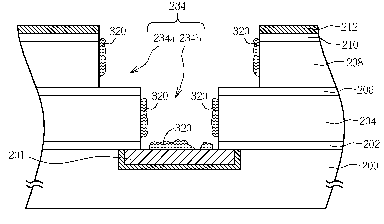
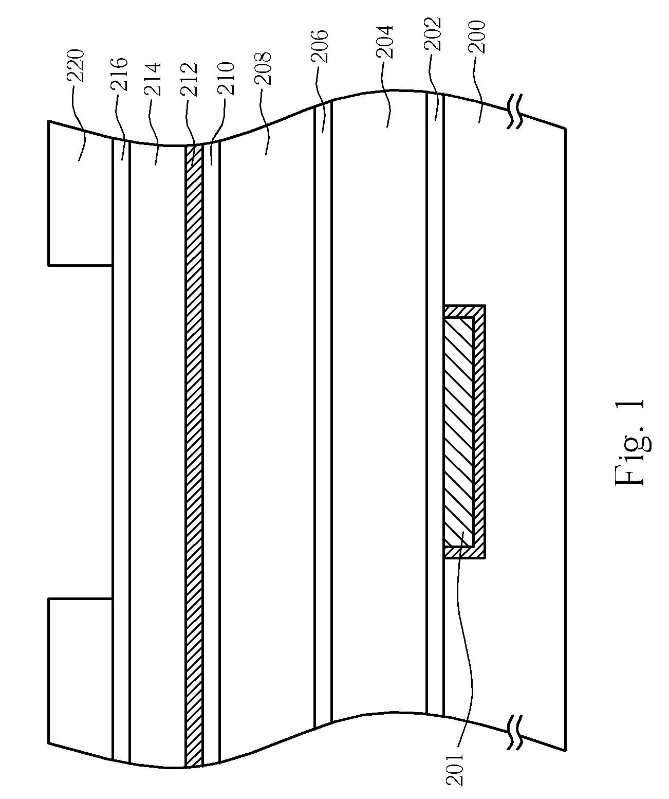
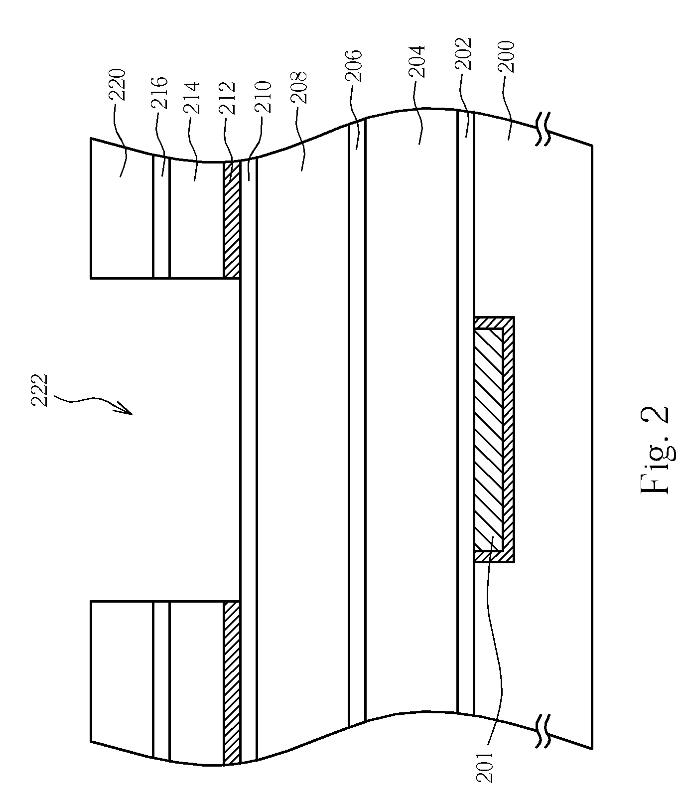
[0018]The present invention pertains to an improved method for effectively removing post-etch residues in a trench / via opening or through hole, which is etched into low-k dielectric film(s) with at least one metal layer as a hard mask for the etching of the through hole. Since a metal hard mask is newly introduced into the damascene processes, it is believed that the resultant post-etch residues would have a newly formulated composition such as complex organic metal compounds that are not possible to be eliminated by virtue of the traditional dry-wet-dry or dry-wet process.

[0019]According to the present invention, a wet-dry-wet process is proposed to effectively removing the post-etch residues from the wafer. More specifically, the present invention discloses a wet-dry-wet process comprising a first wet treatment, followed by an aggressive oxidizing plasma treatment, then a reducing plasma treatment, and finally a second wet treatment. Both the first and second wet treatments involv...


PUM

PropertyMeasurementUnit
temperatureaaaaaaaaaa
thicknessaaaaaaaaaa
dielectric constantaaaaaaaaaa

Abstract

A low-k dielectric film is deposited on the wafer. A metal layer is then deposited over the low-k dielectric film. A resist pattern is formed over the metal layer. The resist pattern is then transferred to the underlying metal layer to form a metal pattern. The resist pattern is stripped off. A through hole is plasma etched into the low-k dielectric film by using the metal pattern as a hard mask. The plasma etching causes residues to deposit within the through hole. A first wet treatment is then performed to soften the residues. A plasma dry treatment is carried out to crack the residues. A second wet treatment is performed to completely remove the residues.

Description

BACKGROUND OF INVENTION[0001]1. Field of the Invention[0002]The present invention relates to the field of semiconductor fabrication and, more particularly, to a method for removing post-etch residues in a trench / via opening, which is etched into low-k dielectric films with at least one metal layer as a hard mask.[0003]2. Description of the Prior Art[0004]As pitches between interconnection wirings of integrated circuits shrink to very deep sub-micron scale or beyond, post-etch trench / via residual looms as a major issue regarding the success in damascene or dual damascene processes. Several prior arts have addressed this problem.[0005]For example, U.S. Pat. No. 6,797,627 filed Dec. 5, 2001 to Shih et al. discloses a dry-wet-dry solvent-free process for removing polymer residuals, which are allegedly mixed with copper oxide substances, from the damascened trench / via bottom and sidewalls. The proposed method is carried out after the nitride or carbide cap layer exposed by the via openin...

Claims


Application Information

Patent Timeline
Patent Type & Authority Patents(United States)
IPC IPC(8): H01L21/302H01L21/461
CPCH01L21/02063H01L21/31144H01L21/76814H01L21/76811Y10S438/963Y10S438/906
Inventor WENG, CHENG-MINGLIN, MIAO-CHUNHUANG, CHUN-JEN
Owner UNITED MICROELECTRONICS CORP
Why Eureka
Try Eureka