Method and resistive bridge circuit for the detection of solder-joint failures in a digital electronic package

a resistive bridge and solder-joint technology, applied in the direction of soldering apparatus, semiconductor/solid-state device testing/measurement, instruments, etc., can solve the problem achieve the effect of increasing the detection voltage, noise tolerance and detection sensitivity

Inactive Publication Date: 2007-03-27
RIDGETOP GROUP
View PDF11 Cites 19 Cited by
  • Summary
  • Abstract
  • Description
  • Claims
  • Application Information

AI Technical Summary

Benefits of technology

[0011]The present invention provides a simple, inexpensive and low power method and circuit for monitoring 24-7 the integrity of solder-joint networks from the internal die connections to the external package connections during normal operation of digital electronic packages, such as FPGAs or microcontrollers. The invention is particularly applicable to high density ball grid array (BGA) packages.
[0013]A detector compares the detection voltage to the sensitivity voltage and outputs a Pass / Fail signal for the solder-joint network. If the network is healthy, its effective resistance, hence the voltage at the R3 / RSJ junction will be low and the detector will indicate a Pass. However, if a fault occurs anywhere in the network, it is as though a high-value resistor was switched into the solder joint network, which has the effect of increasing the detection voltage. When the network resistance exceeds a nominal trigger value, the detection voltage becomes high enough to switch the fault detector causing it to indicate a Fail. Supply noise is both attenuated and partially rejected in the common mode. Proper selection of R1 and R2 allows for the establishment of the desired noise sensitivity (to prevent false positives) and the detection of small network resistances as failures. Both aspects are important for providing reliable detection in an operating package that has noisy supplies and buffers and for detecting small increases in network resistance that are precursors for network failure. By connecting the resistive bridge between the high and low supply voltages and one side of the solder-joint network to the low supply voltage, both noise tolerance and detection sensitivity can be achieved without drawing an unacceptable amount of power for the detection circuit.

Problems solved by technology

However, if a fault occurs anywhere in the network, it is as though a high-value resistor was switched into the solder joint network, which has the effect of increasing the detection voltage.

Method used


Image

  • Method and resistive bridge circuit for the detection of solder-joint failures in a digital electronic package
  • Method and resistive bridge circuit for the detection of solder-joint failures in a digital electronic package
  • Method and resistive bridge circuit for the detection of solder-joint failures in a digital electronic package

Examples


Embodiment Construction

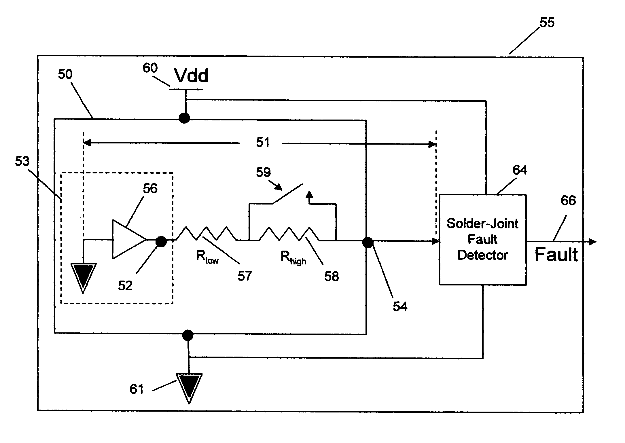
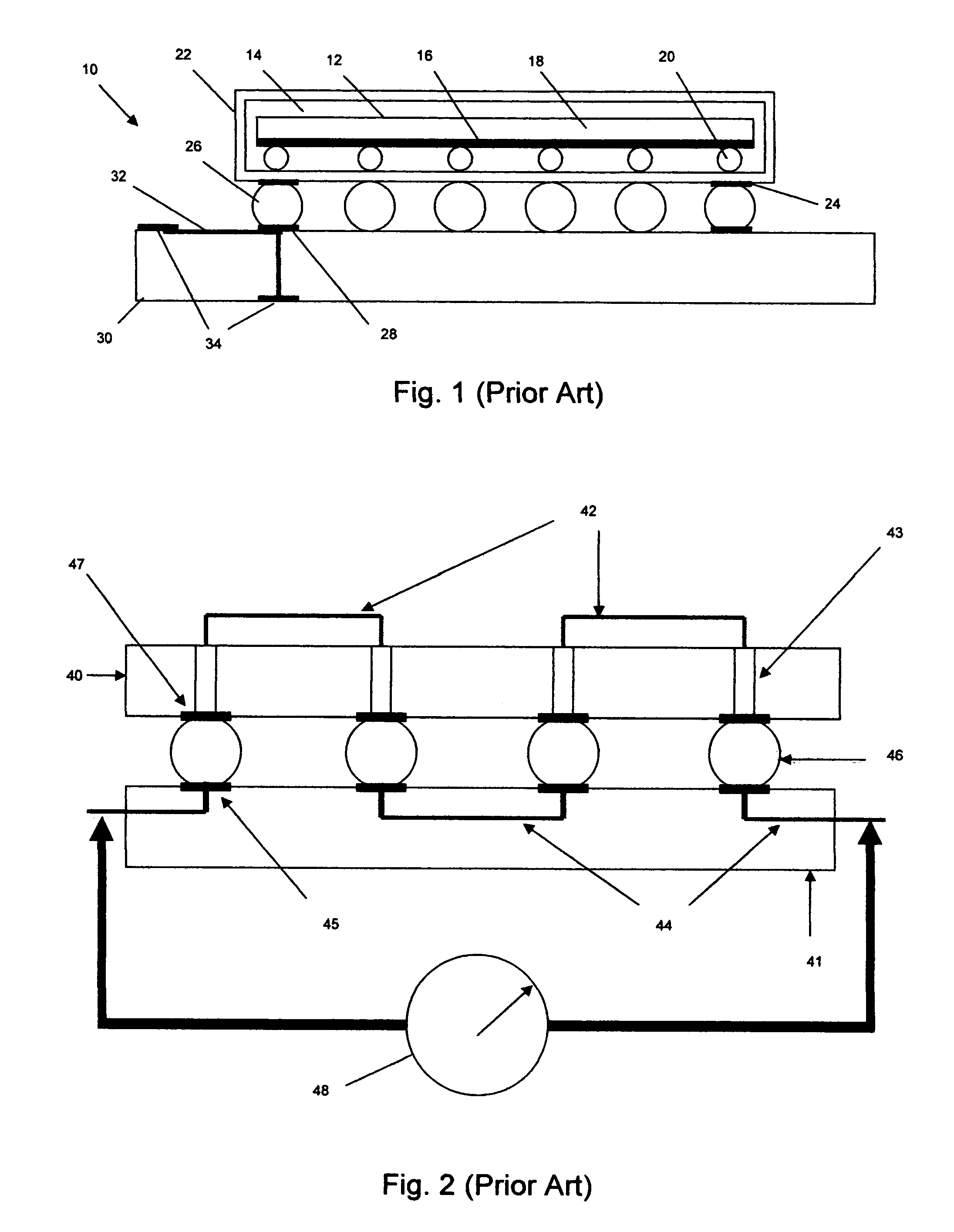
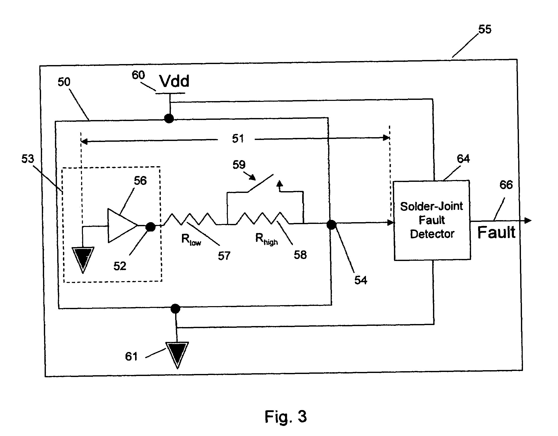
[0024]The present invention provides a method for evaluating solder-joint integrity of operational digital electronic packages, such as FPGAs or Microcontrollers that have internal and external solder-joint connections, and particularly for evaluating the integrity of the solder-joint network during normal operation of the digital electronic packages. The invention will be described for a FPGA including a flip-chip mounted in a BGA package that is soldered to a PWB in which the solder-joint network includes a mechanical connection at the output of an I / O buffer on the die, a number of other internal mechanical connections or solder-joints and an external solder-joint between the package and PWB. But it will be understood that the method and circuit for evaluating solder-joint integrity is generally applicable to any digital electronic package that has a mechanical connection on the die regardless of whether the die is configured as an FPGA, microcontroller or otherwise, or whether a...


PUM

PropertyMeasurementUnit
voltageaaaaaaaaaa
voltageaaaaaaaaaa
sensitivity voltageaaaaaaaaaa

Abstract

A solder-joint detection circuit uses a resistive bridge and a differential detector to detect faults in the solder-joint network both inside and outside the digital electronic package during operation. The resistive bridge is preferably coupled to a high supply voltage used to power the package. Resistors R1 and R2 are connected in series at a first junction between the high and low supply voltages and a resistor R3 is coupled to the high supply voltage and connected in series with the resistance of the solder-network at a second junction. The network is held at a low voltage on the die. The detector compares the sensitivity and detection voltages and outputs a Pass / Fail signal for the solder-joint network.

Description

CROSS-REFERENCE TO RELATED APPLICATIONS[0001]This application claims benefit of priority under 35 U.S.C. 119(e) to U.S. Provisional Application Nos. 60 / 657,101 entitled “Non-Invasive Real Time Method for the Detection of Solder Joint Failures” filed on Feb. 28, 2005 and 60 / 737,848 entitled “Real-Time, In-Situ Method for the Detection of Solder-Joint Fatigue Damage Using the Solder Joint as a Resistive Switch” filed on Nov. 18, 2005, the entire contents of which are incorporated by reference.Governmental Rights[0002]This invention was made with Government support under Contract N6833505-C-0101 awarded by Naval Air Warfare Center AD (LKE). The Government has certain rights in this invention.BACKGROUND OF THE INVENTION[0003]1. Field of the Invention[0004]This invention relates to a method and circuit for detection of failures in the solder-joint networks in digital electronic packages such as Field Programmable Gate Arrays (FPGAs) and Microcontrollers and between the package's ball gri...

Claims


Application Information

Patent Timeline
Patent Type & Authority Patents(United States)
IPC IPC(8): H05B1/02
CPCB23K1/0016G01R31/048G01R31/2884B23K2201/40B23K2101/40G01R31/71H01L2224/16225H01L2924/00011H01L2924/00014H01L2924/15311H01L2224/0401
Inventor HOFMEISTER, JAMES P.SPUHLER, PHILIPP S.VERMEIRE, BERT M.
Owner RIDGETOP GROUP
Why Eureka
Try Eureka