Liquid crystal device, projection type display and electronic equipment

a liquid crystal display and projection type technology, applied in the field of liquid crystal devices, can solve the problems of reducing the aperture ratio as a display system, the distance between pixels, and the image roughness to become remarkable, so as to reduce the disclination of the display, minimize or prevent the production of disclination defects, and achieve high contrast and bright display

Inactive Publication Date: 2007-03-27
138 EAST LCD ADVANCEMENTS LTD
View PDF43 Cites 15 Cited by
  • Summary
  • Abstract
  • Description
  • Claims
  • Application Information

AI Technical Summary

Benefits of technology

[0013]The present invention addresses the above-described problems, and an object of the invention is to provide a liquid crystal device, a projection type display system, and electronic equipment in which display defects caused by disclination are reduced, minimized or prevented from being produced for a highly fine liquid crystal display system with a space between pixels made to become narrow to make it possible to provide a high-contrast and bright display.

Problems solved by technology

When using the liquid crystal display system as the projection type system, an increase in magnification with a previous pixel number causes image roughness to become remarkable.
This causes an increase in an area of a black matrix covering the above portion to reduce a pixel opening area contributing to the display, which causes a problem of reducing an aperture ratio as a display system.
However, even with advent of such various kinds of projection type display systems, in a high resolution liquid crystal panel, a distance between pixels, that is, a distance between pixel electrodes, becomes small.
Thus, the high resolution liquid crystal panel has a problem in that an a pixel is affected by a transverse electric field from peripheries of other adjacent pixel electrodes, which causes disclination of the liquid crystal to produce defects in a display region.
This causes a problem of producing linear display defects, called disclination lines, at a boundary region with the liquid crystals with the orientating directions being subtly different.
The problem of the display defects due to such a transverse electric field occurs not only in the projection type display system, but also in a highly fine direct-vision type liquid crystal device.
However, the liquid crystal devices proposed in Japanese Patent Laid-Open No. 202356 / 1999 relate to transmission type liquid crystal devices, whose respective conditions and structures can only be applied to a transmission type liquid crystal device.

Method used


Image

  • Liquid crystal device, projection type display and electronic equipment
  • Liquid crystal device, projection type display and electronic equipment
  • Liquid crystal device, projection type display and electronic equipment

Examples


first embodiment

(First Embodiment)

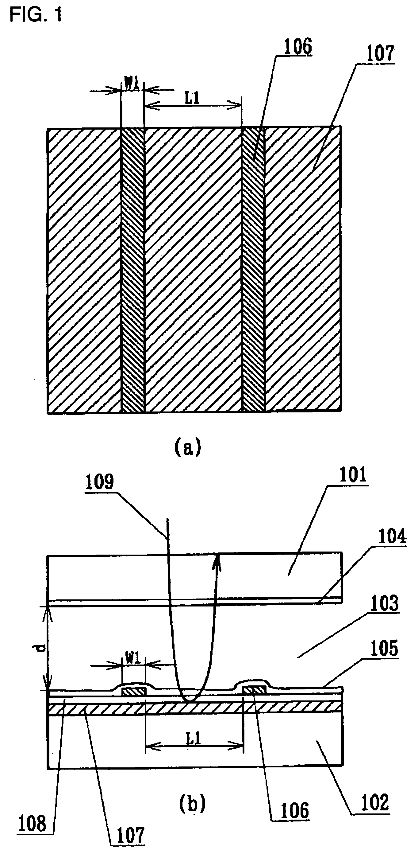
[0108]FIGS. 1(a) and 1(b) are schematics showing a structure of a first embodiment of a liquid crystal device according to the invention. FIG. 1(a) is a front view of one pixel, and FIG. 1(b) a cross sectional view thereof. A structure is provided in which a liquid crystal layer 103 is disposed between two substrates, an upper substrate 101 and a lower substrate 102. The upper substrate 101 has an alignment layer 104 formed on the inner face thereof. On the inner side of the lower substrate 102, there are formed a second electrode 107, an insulation film 108 including SiOx, a first electrode 106 and an alignment layer 105.

[0109]The first electrode 106 is a linear transparent electrode and the second electrode 107 is a rectangular reflecting electrode. The second electrode 107 reflects light 109 incident from the upper substrate 101 side. The liquid crystal layer 103 is controlled by an external driving circuit with an electric field produced due to an electric pote...

second embodiment

(Second Embodiment)

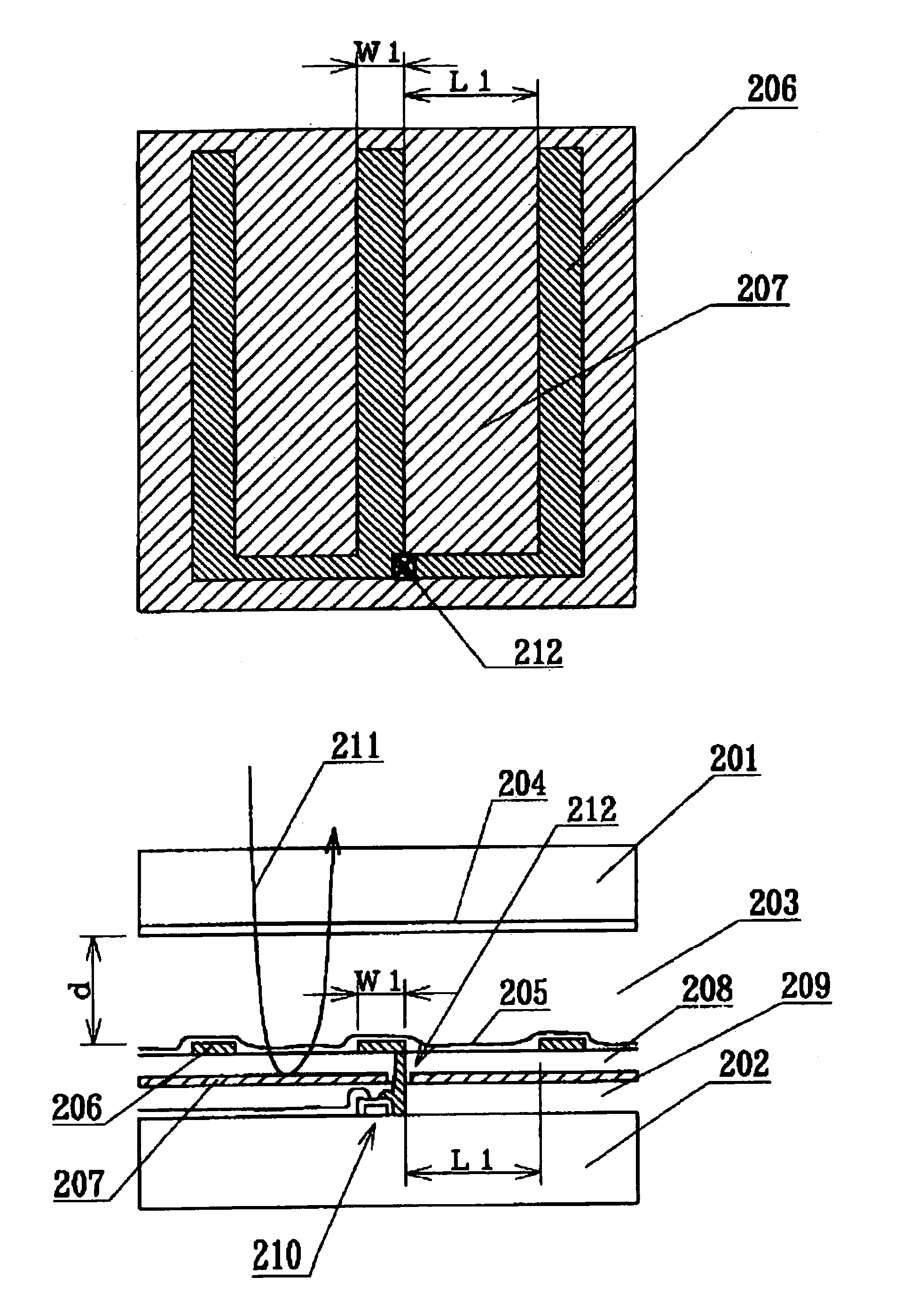
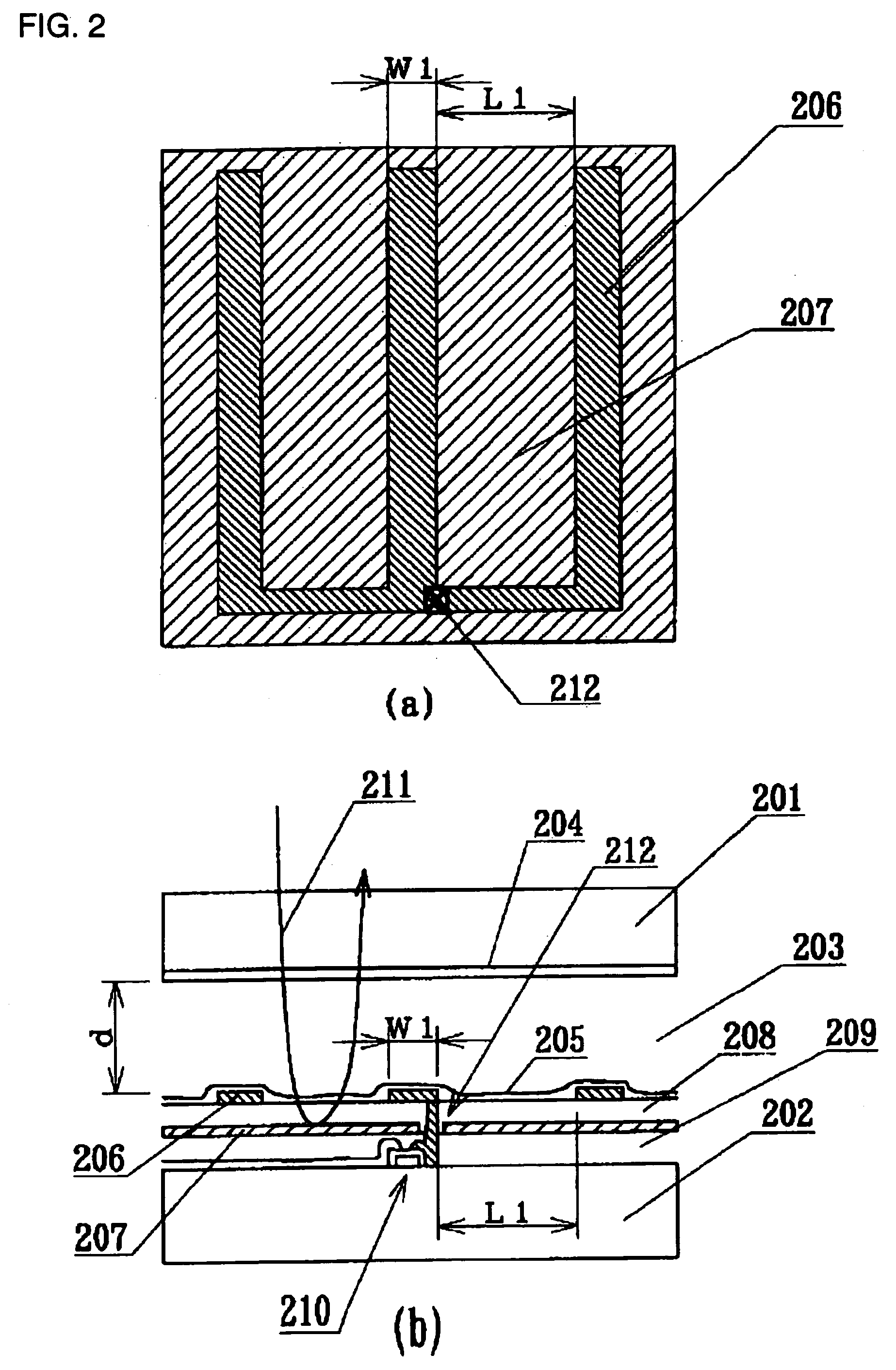
[0118]FIGS. 2(a) and 2(b) are schematics showing a structure of a second embodiment of a liquid crystal device according to the invention. FIG. 2(a) is a front view of one pixel, and FIG. 2(b) is a cross sectional view thereof. A structure is provided in which a liquid crystal layer 203 is disposed between two substrates, an upper substrate 201 and a lower substrate 202. The upper substrate 201 has an alignment layer 204 formed on the inner face thereof. On the inner side of the lower substrate 202, there are formed a scanning signal line, an image signal line and a TFT element 210, over which there are further formed a first insulation film 209, a common electrode 207, a second insulation film 208, a pixel electrode 206, and an alignment layer 205 in order. In the common electrode 207, there is provided an opening (contact hole) 212 for making the TFT element 210 and the pixel electrode 206 to be in contact with each other. The pixel electrode 206 is a linear tra...

third embodiment

(Third Embodiment)

[0122]In the reflection type liquid crystal device shown in FIG. 2, an electrode width of the pixel electrode 206 and an interelectrode space of the pixel electrode 206 are defined as W1 and L1, respectively. Here, there was studied the relationship between the ratio of the interelectrode space L1 of the pixel electrode 206 to the electrode width W1 of the pixel electrode 206 (L1 / W1) and the reflectance of the reflection type liquid crystal device. The upper row of TABLE 1 shows the results in the case where the pixel electrode 206 is provided as the reflecting electrode, and the lower row shows the results in the case where the common electrode 207 is provided as the reflecting electrode.

[0123]

TABLE 1L1 / W10.0010.0050.0510.1040.2010.5051.102REFLECTANCE49.973.573.470.559.855.845.8OF LIQUIDCRYSTALDEVICE (%)L1 / W13.99810.00515.10220.19240.00262.511REFLECTANCE59.977.385.673.562.355.1OF LIQUIDCRYSTALDEVICE (%)

[0124]According to the upper row of TABLE 1, when L1 / W1 is equ...


PUM

PropertyMeasurementUnit
thicknessaaaaaaaaaa
widthaaaaaaaaaa
distanceaaaaaaaaaa

Abstract

The invention provides a reflection type liquid crystal device, and a projection type display and electronic equipment in which display defects caused by disclination are reduced, minimized or prevented from being produced for a highly fine liquid crystal display with a space between pixels made to be narrow to make it possible to provide a high-contrast and bright display. A liquid crystal device includes a liquid crystal layer sandwiched between a first substrate and a second substrate, and a first electrode and a second electrode formed on a face of the above-described second substrate on a side of the above-described liquid crystal layer. The above-described first electrode and the above-described second electrode are formed so that an electric field substantially parallel to the surface of the substrate with respect to the above-described liquid crystal layer can be applied thereto. The above-described first electrode is formed in a linear shape having a specified line width on the above-described second electrode with a second insulation film interposed therebetween. The above-described second electrode is formed in a rectangular shape, and at least one of the above-described first electrode and the above-described second electrode is a reflecting electrode that causes incident light coming from a direction of the above-described first substrate.

Description

[0001]This is a Division of application Ser. No. 10 / 086,529 filed Mar. 4, 2002 now U.S. Pat. No. 6,784,966. The entire disclosure of the prior application is hereby incorporated by reference herein in its entirety.BACKGROUND OF THE INVENTION[0002]1. Field of Invention[0003]The present invention relates to a liquid crystal device, and more particularly to a liquid crystal device that utilizes a transverse electric field. The invention also relates to a projection type display system and electronic equipment using the liquid crystal device.[0004]2. Description of Related Art[0005]Liquid crystal display systems have long been the subject of increasing demand as not only a direct-vision type, but also a projection type display element of an apparatus, such as a projection television. When using the liquid crystal display system as the projection type system, an increase in magnification with a previous pixel number causes image roughness to become remarkable. Thus, in order to obtain a ...

Claims


Application Information

Patent Timeline
Patent Type & Authority Patents(United States)
IPC IPC(8): G02F1/1343G02F1/1337G02F1/1362
CPCG02F1/134363G03B21/00G02F1/133553G02F1/136227G02F2001/134318G02F2201/40G02F2203/02G02F2001/13373G03B21/006G02F1/13373
Inventor MAEDA, TSUYOSHIOZAWA, KINYAOKUMURA, OSAMUOKAMOTO, EIJIKAWATA, HIROTAKAMATSUSHIMA, TOSHIHARUSEKI, TAKUMIKAMIJO, KIMITAKA
Owner 138 EAST LCD ADVANCEMENTS LTD
Why Eureka
Try Eureka