Method of locating sub-resolution assist feature(s)

a technology of assist feature and sub-resolution, which is applied in the direction of photomechanical treatment originals, instruments, nuclear engineering, etc., can solve the problems of limiting various aspects of semiconductor design, limiting the size scale of masks, and limiting the resultant wafer circuit limitations,

Active Publication Date: 2007-04-03
TEXAS INSTR INC
View PDF17 Cites 180 Cited by
  • Summary
  • Abstract
  • Description
  • Claims
  • Application Information

AI Technical Summary

Problems solved by technology

In this manner, therefore, limitations on the mask may be at a larger size scale than on the wafer, due to the use of the reducer lens.
Given the use of imaging and masks as discussed above, various aspects of semiconductor design are necessarily limited by constraints of the mask and its related technology.
In other words, since the mask defines the image that passes through it and that ultimately dictates the layout of the circuit on the wafer, then limitations of the mask represent limitations of the resultant wafer circuit.
More specifically, it has been determined that if such neighboring features are too closely formed, then the features cannot be resolved optically with conventional light source and mask techniques, causing an undesirable or unacceptable image on the wafer.
Such limitations are particularly evident when a desired dimension of a wafer feature is smaller than the wavelength of the light that passes through the mask.
As a result, there is overlap between the non-phase shifted and phase shifted light, causing light interference that effectively cancels some of the overlapping light and produces a clearer edge for the resulting wafer feature.
In view of the above, with assist (or SRAF) technology comes the complexity of a methodology for locating the assist features on the mask or reticle.
Thus, the prior art provides drawbacks in its limitations of achieving only certain primary feature definition and minimal wafer feature sizes, while the preferred embodiments improve upon these limitations as demonstrated below.

Method used


Image

  • Method of locating sub-resolution assist feature(s)
  • Method of locating sub-resolution assist feature(s)
  • Method of locating sub-resolution assist feature(s)

Examples


Embodiment Construction

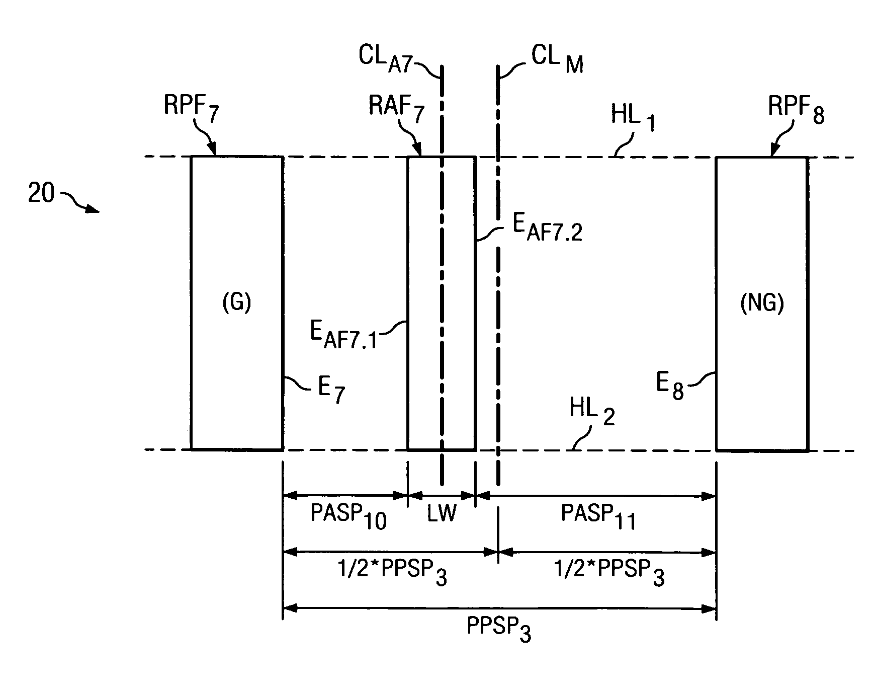
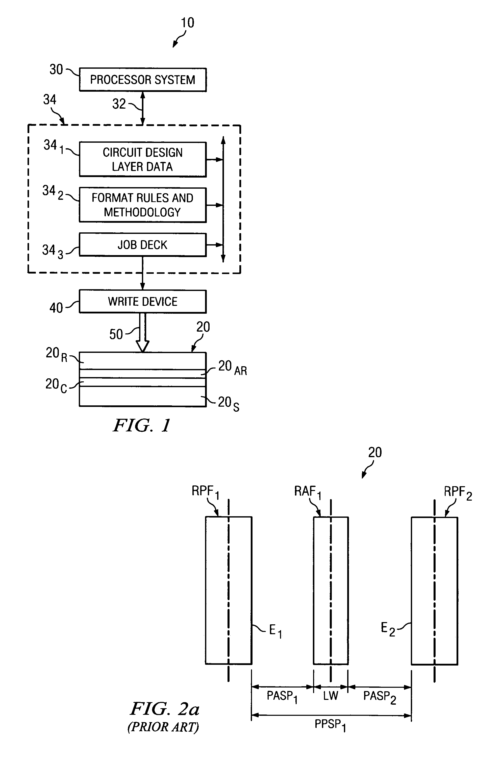
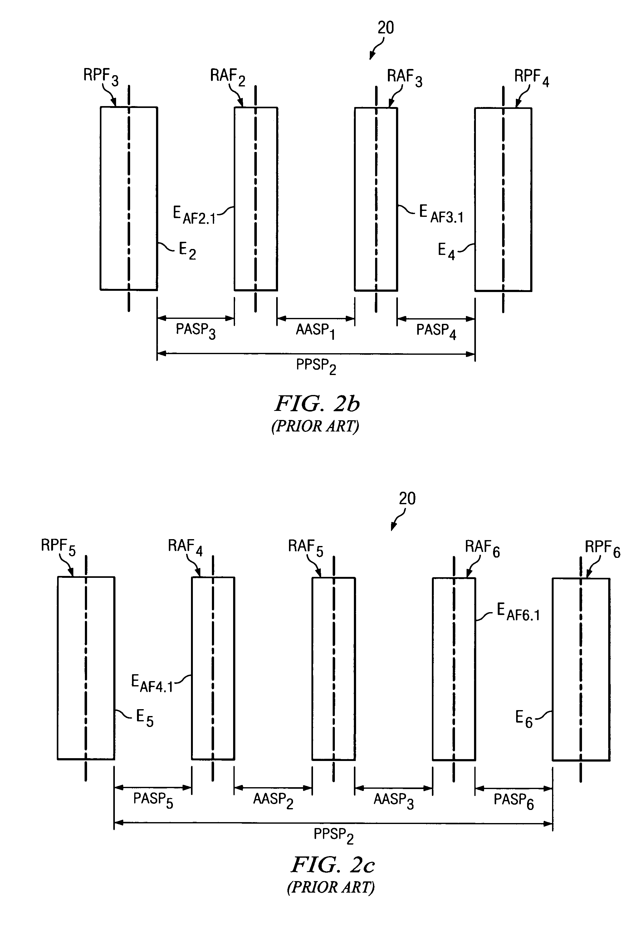
[0021]FIG. 1 illustrates a block diagram of a system 10 for forming a reticle 20 in accordance with the preferred embodiments. By way of introduction, the general nature of system 10 is known in the art, but novel aspects are added thereto and improve reticle 20 for reasons appreciated throughout the remainder of this document.

[0022]Looking then to system 10 in general, it includes a processor system 30 that may be embodied in various different forms of hardware and software, typically including one or more processors and / or computing devices. Processor system 30 has one or more interfaces 32 coupled to a data store 34, where data store 34 represents any of various forms of storage such as drives and memory, and where such storage may retain program or other data that may be read / written with respect to processor system 30. Data store 34 is shown to provide two input data files 341 and 342 via interface 32 to processor system 30, and to receive an output data field 343 from processo...


PUM

PropertyMeasurementUnit
widthaaaaaaaaaa
widthaaaaaaaaaa
widthaaaaaaaaaa

Abstract

A method of operating a computing system to determine reticle data. The reticle data is for completing a reticle for use in projecting an image to a semiconductor wafer. The method receives circuit design layer data comprising a desired circuit layer layout, and the layout comprises a plurality of lines. The method also identifies in the plurality of lines a first line portion for use as a first circuit function and a second line portion for use as a second circuit function that differs from the first circuit function. The first line portion is parallel and adjacent to the second line portion. The method also provides the reticle data in an output data file for use in forming features on the reticle. The method also indicates parameters for forming first and second primary features as well as at least one assist feature on the reticle having an area between the first primary feature and the second primary feature, wherein in use of the reticle for use in projecting the image to the semiconductor wafer the area will favor greater assistance to the first primary feature as compared to the second primary feature.

Description

CROSS-REFERENCES TO RELATED APPLICATIONS[0001]This application claims priority under 35 U.S.C. § 119 of U.S. Provisional Application No. 60 / 655,956, filed Feb. 24, 2005.STATEMENT REGARDING FEDERALLY SPONSORED RESEARCH OR DEVELOPMENT[0002]Not Applicable.BACKGROUND OF THE INVENTION[0003]The present embodiments relate to forming semiconductor circuit wafers and are more particularly directed to locating sub-resolution assist features (“SRAF”) on a mask (or reticle) for use with such wafers.[0004]The history and prevalence of semiconductor devices are well known and have drastically impacted numerous electronic devices. As a result and for the foreseeable future, successful designers constantly are improving the semiconductor fabrication process, and improvements are in numerous areas including device size, fabrication efficiency, and device yield. The present embodiments advance these and other goals by improving the methodology for developing parameters to implement sub-resolution ass...

Claims


Application Information

Patent Timeline
Patent Type & Authority Patents(United States)
IPC IPC(8): G06F17/50G03F1/00G06F19/00G21K5/00
CPCG03F1/36G03F1/144G03F1/70
Inventor ZHANG, GUOHONGO'BRIEN, SEAN
Owner TEXAS INSTR INC
Why Eureka
Try Eureka