Delay locked loop and semiconductor memory device having the same

Inactive Publication Date: 2007-04-10
SAMSUNG ELECTRONICS CO LTD
View PDF9 Cites 24 Cited by
  • Summary
  • Abstract
  • Description
  • Claims
  • Application Information

AI Technical Summary

Benefits of technology

[0010]It is an object of the present invention to provide a delay locked loop which can generate a plurality of clock signals which have a precise phase difference of 90° by offsetting transient phase change (noise) resulting from variation of power voltage.
[0011]It is another object of the present invention to provide a semiconductor memory device having a delay locked loop which can generate a plurality of clock signals which precisely have a precise phase difference of 90° by offsetting transient phase change (noise) resulting from variation of power voltage.

Problems solved by technology

However, the clock signals CLK0, CLK90, CLK180, and CLK270 generated from the conventional delay locked loop might not have an precise phase difference of 0°, 90°, 180°, and 270° due to transient phase change (noise) which results from variation of power voltage and external noise that occurs during operation.

Method used


Image

  • Delay locked loop and semiconductor memory device having the same
  • Delay locked loop and semiconductor memory device having the same
  • Delay locked loop and semiconductor memory device having the same

Examples


Embodiment Construction

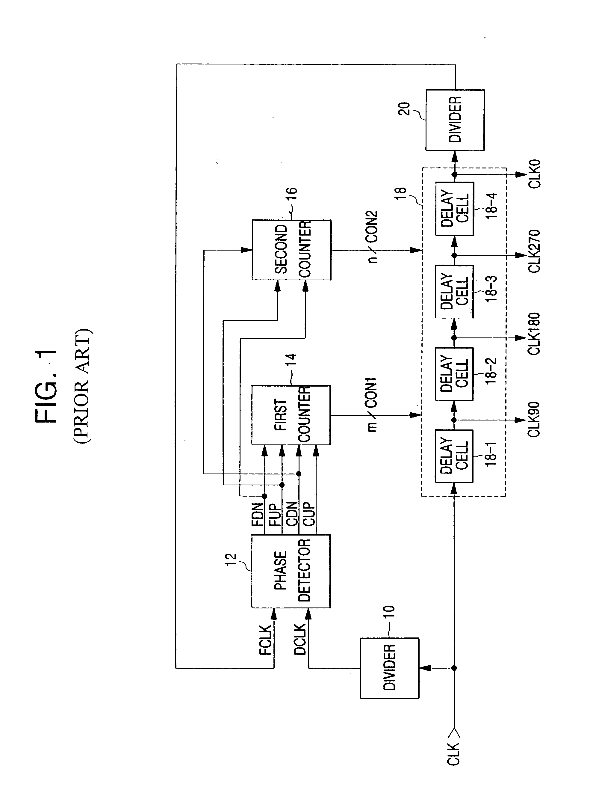
[0034]The present invention will now be described more fully hereinafter with reference to the accompanying drawings, in which preferred embodiments of the invention are shown. This invention may, however, be embodied in different forms and should not be construed as limited to the embodiments set forth herein. Rather, these embodiments are provided so that this disclosure will be thorough and complete, and will fully convey the scope of the invention to those skilled in the art. In the drawings, the thickness of layers and regions are exaggerated for clarity. Like numbers refer to like elements throughout the specification.

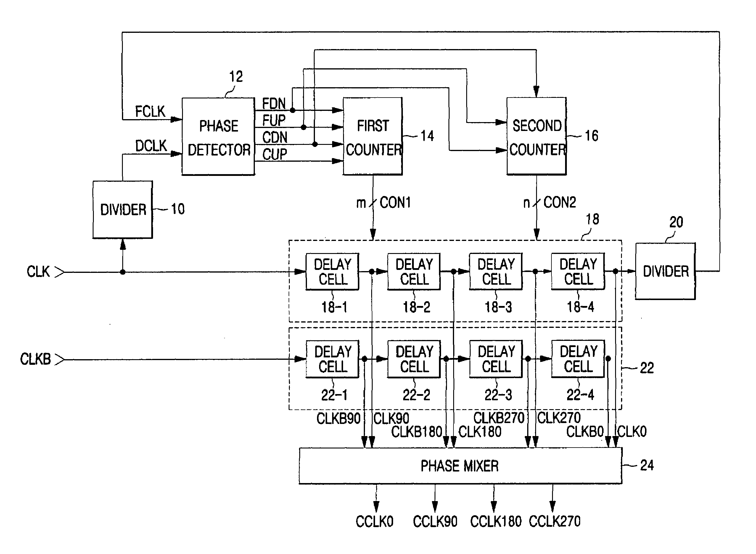
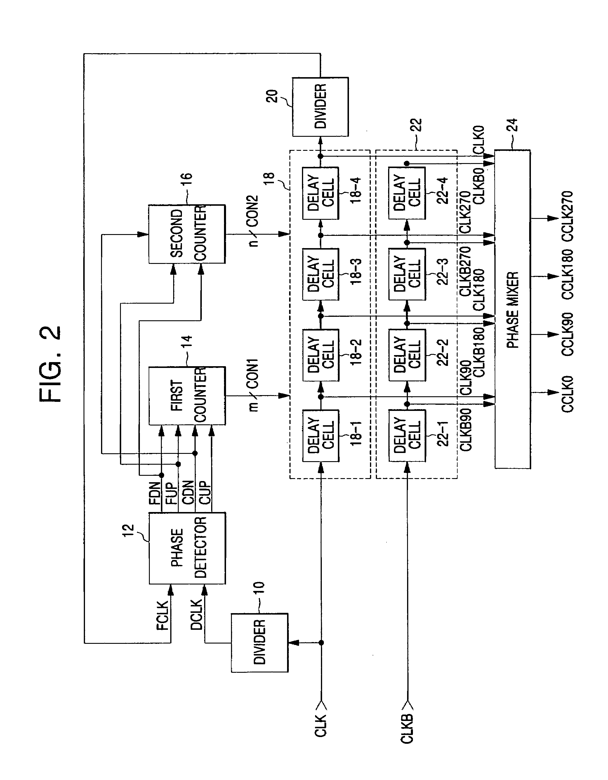
[0035]FIG. 2 is a block diagram illustrating a delay locked loop according to an embodiment of the present invention. The delay locked loop of FIG. 2 further includes a delay circuit 22 and a phase mixer 24 in addition to configuration of FIG. 1. The delay circuit 22 includes delay cells 22-1 to 22-4 connected in a cascade configuration.

[0036]Like reference numer...


PUM


Abstract

In a delay locked loop and a semiconductor memory device having the same, the delay locked loop includes a phase detecting and control signal generator for detecting a phase difference between a clock signal and a feedback clock signal and generating a plural-bit delay control signal which varies according to the phase difference; a first delay having a predetermined number of first delay cells which are cascade-connected for delaying the clock signal to generate a plurality of output clock signals and the feedback clock signal in response to the plural-bit delay control signal; a second delay having a predetermined number of second delay cells which are cascade-connected for delaying an inverted clock signal to generate a plurality of inverted output clock signals in response to the plural-bit delay control signal; and a phase mixer for phase-mixing corresponding clock signals among the plurality of output clock signals and the plurality of inverted output clock signals to output a plurality of corrected output clock signals.

Description

CROSS-REFERENCE TO RELATED APPLICATION[0001]This application claims the benefit of Korean Patent Application No. 2004-90599, filed Nov. 8, 2004, the disclosure of which is hereby incorporated herein by reference in its entirety.BACKGROUND OF THE INVENTION[0002]1. Field of the Invention[0003]The present invention relates to a delay locked loop and, more particularly, to a delay locked loop which can generate a plurality of clock signals which have different phases from each other and a semiconductor memory device having the same.[0004]2. Description of the Related Art[0005]A delay locked loop is commonly employed in a control device and a semiconductor memory device to generate a plurality of clock signals which have different respective phases. Each device generates data strobe signals at a higher rate higher than externally applied clock signals using a plurality of clock signals generated from the delay locked loop and receives or outputs data in response to the data strobe signal...

Claims


Application Information

Patent Timeline
Patent Type & Authority Patents(United States)
IPC IPC(8): H03K7/00
CPCH03L7/0805H03L7/0814H03L7/0818H03L7/0816G11C7/1051G11C7/22H03L7/085
Inventor JEON, YOUNG-JIN
Owner SAMSUNG ELECTRONICS CO LTD
Why Eureka
Try Eureka