

Optical semiconductor device
a technology of optical semiconductor and semiconductor device, which is applied in the direction of semiconductor device, semiconductor/solid-state device details, electrical apparatus, etc., can solve the problems of complicated procedures for incorporating optical semiconductor devices into electronic equipment, and achieve the effects of improving the ability to prevent faulty operation of ic chip(s), improving optical shielding, and preventing deformation of the terminal region
- Summary
- Abstract
- Description
- Claims
- Application Information
AI Technical Summary
Benefits of technology
Problems solved by technology
Method used
Image

Examples
embodiment 1
[0034
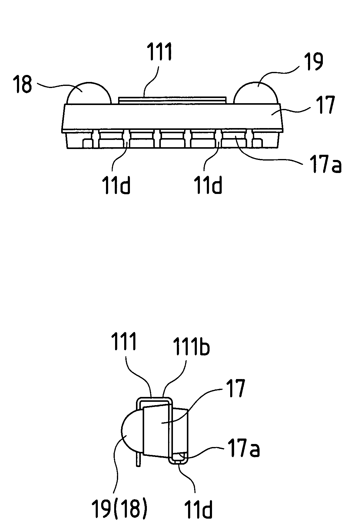
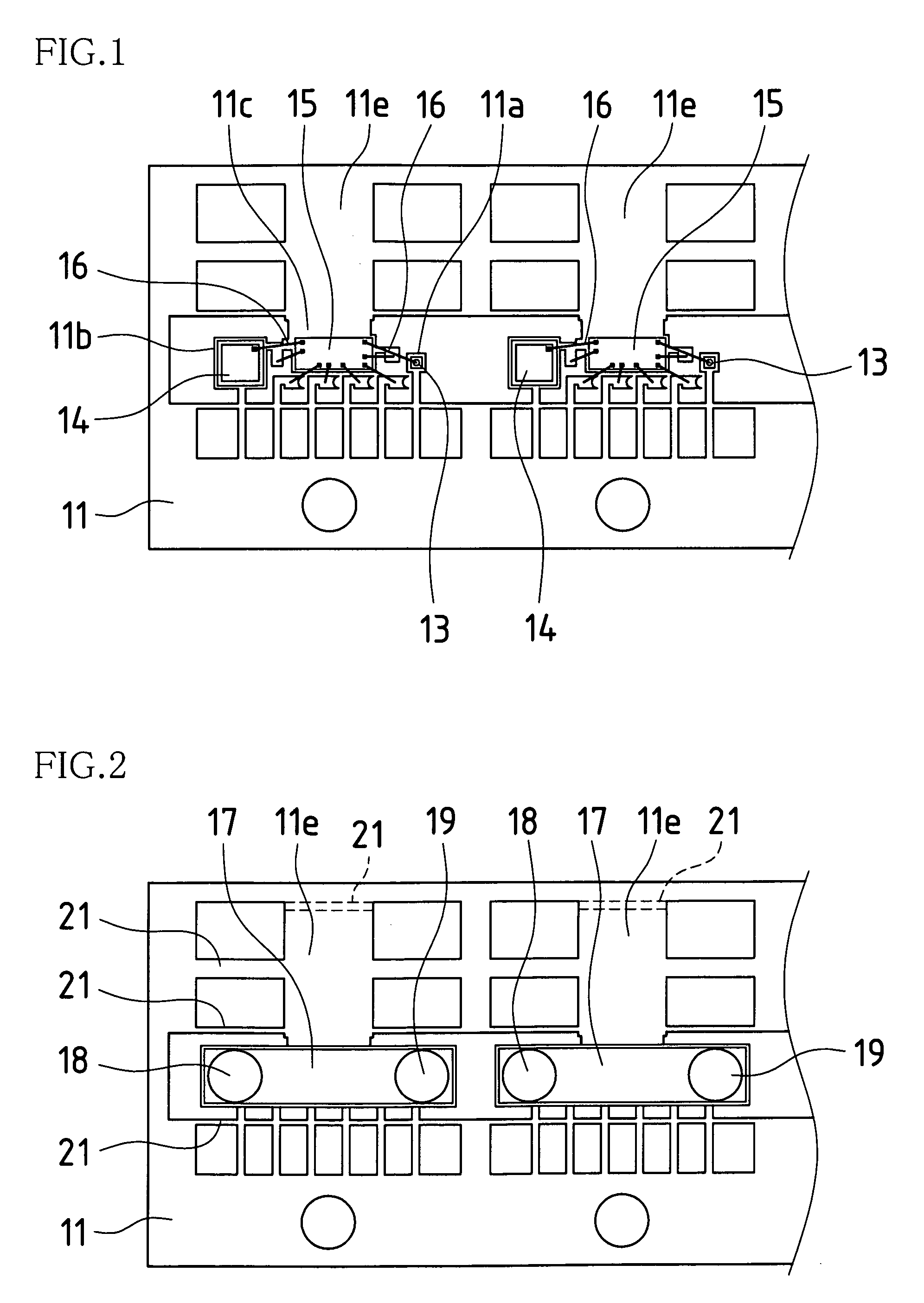
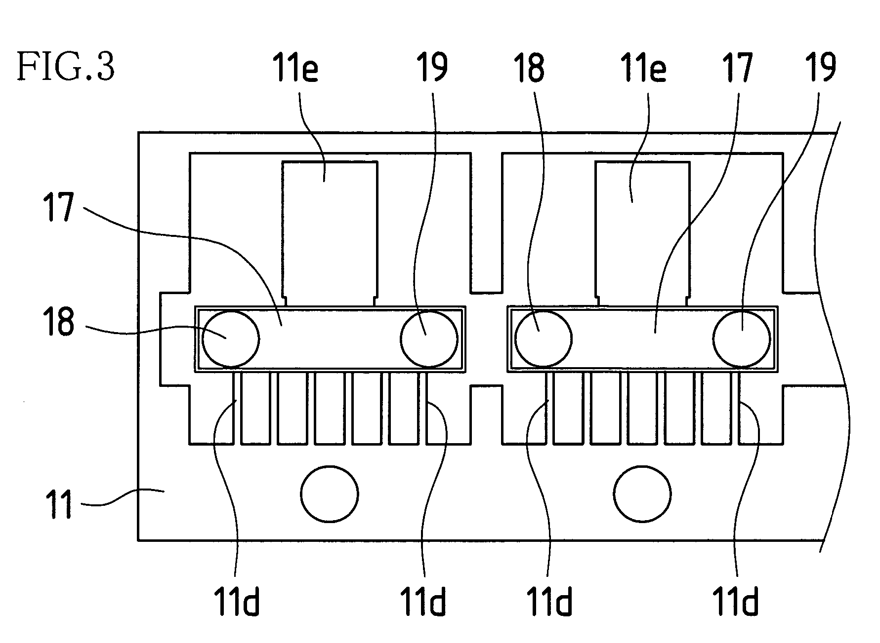
[0035]FIGS. 1 through 3 are plan views showing stages during the course of manufacture of an optical semiconductor device associated with the present first embodiment; FIG. 4(a) is a plan view of an optical semiconductor device associated with the present first embodiment; FIG. 4(b) is a front view of an optical semiconductor device associated with the present first embodiment; and FIG. 4(c) is a side view of an optical semiconductor device associated with the present first embodiment.
[0036]At the optical semiconductor device of the present first embodiment, lead frame portion(s) 11e, serving as shield case region(s) 111, has or have been created in advance in such fashion as to extend from component mounting region(s) 11c of lead frame(s) 11, at which signal processing IC chip(s) 15 is / are installed.
[0037]Light-emitting element(s) 13, light-receiving element(s) 14, and signal processing IC chip(s) 15 are respectively bonded by means of electrically conductive resin (not shown)...
embodiment 2
[0041
[0042]FIGS. 5 and 6 are plan views showing stages during the course of manufacture of an optical semiconductor device associated with the present second embodiment; FIG. 7(a) is a plan view of an optical semiconductor device associated with the present second embodiment; FIG. 7(b) is a front view of an optical semiconductor device associated with the present second embodiment; and FIG. 7(c) is a side view of an optical semiconductor device associated with the present second embodiment.
[0043]In making the optical semiconductor device of the present second embodiment, light-emitting element(s), light-receiving element(s), and signal processing IC chip(s) are respectively bonded by means of electrically conductive resin to respective component mounting region(s) of lead frame(s) 31, electrical connection being thereafter made by means of gold wire or the like (the constitution up to this point being similar to that shown in FIG. 1), following which translucent resin is used to enc...
embodiment 3
[0046
[0047]FIG. 8(a) is a plan view showing a stage prior to encapsulation during the course of manufacture of an optical semiconductor device associated with the present third embodiment; FIG. 8(b) is a plan view showing a stage subsequent to encapsulation during the course of manufacture of an optical semiconductor device associated with the present third embodiment; and FIG. 8(c) is a bottom view showing a stage subsequent to cutting and forming during the course of manufacture of an optical semiconductor device associated with the present third embodiment.
[0048]It is necessary that configuration(s) of shield case region(s) 111 of the present invention be of such dimension(s) as will permit it or they to cover IC chip(s) 15 within resin package(s) 17. In the present case, such dimension(s) being on the order of 2 mm, there is concern that when such portion(s) is / are bent, stress(es) acting at bent region(s) of shield case region(s) 111 will cause occurrence of cracking and / or the...
PUM
 Abstract
Description
Claims
Application Information