Semiconductor integrated circuit device and method for designing the same

Inactive Publication Date: 2007-04-17
SOCIONEXT INC
View PDF7 Cites 0 Cited by
  • Summary
  • Abstract
  • Description
  • Claims
  • Application Information

AI Technical Summary

Benefits of technology

[0006]It is therefore an object of the present invention to provide a semiconductor integrated circuit device in which the power consumption can be reduced, and a method for designing the device. It is another object of the present invention is to provide a semiconductor integrated circuit device in which the power consumption can be reduced without deterioration in the performance thereof, and a method for fabricating the device.

Problems solved by technology

With improvement in the performance of, and increase in the scale of integration of, semiconductor integrated circuit devices, increase in power consumption becomes a serious problem.
In particular, semiconductor integrated circuit devices used in the field of mobile communication operate with limited amounts of power.
However, since the control is performed on every circuit block with the technique described above, it is difficult to further reduce the power consumption in the semiconductor integrated circuit device.
In addition, with the downsizing of elements in the semiconductor integrated circuit device, voltage drop is caused by, for example, an IR-Drop effect, resulting in difficulty in achieving high-speed operation which is a purpose of the semiconductor integrated circuit device.

Method used


Image

  • Semiconductor integrated circuit device and method for designing the same
  • Semiconductor integrated circuit device and method for designing the same
  • Semiconductor integrated circuit device and method for designing the same

Examples


embodiment 1

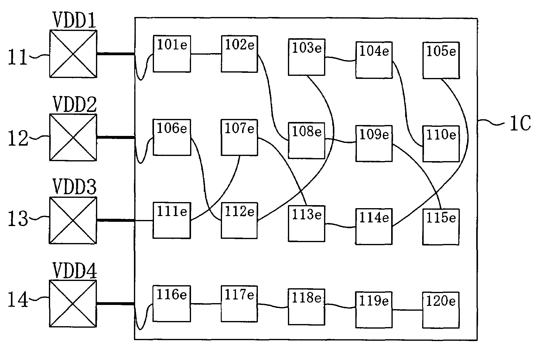
[0088]FIG. 1 is a diagram showing an example of a configuration of a semiconductor integrated circuit device according to a first embodiment of the present invention.

[0089]With respect to the semiconductor integrated circuit device shown in FIG. 1, a circuit block 1C and power supplies 11 through 14 are shown.

[0090]The circuit block 1C includes elements 101e through 120e constituting the block 1C (hereinafter referred to as components). Each of the components 101e through 120e is supplied with one of voltages VDD1 through VDD4 from the respective power supplies 11 through 14 (indicated by bold lines in FIG. 1). FIG. 1 shows that the components 101e through 120e are connected to one another with paths. In this embodiment, the circuit block is a block in a circuit including components such as an AND gate and an OR gate.

[0091]The voltages VDD2 through VDD4 to be supplied to the circuit block 1C are either voltages which have been stepped down at a given rate using the rated voltage VDD...

embodiment 2

[0100]In the following second embodiment of the present invention, as a method for reducing the power consumption by supplying power supply voltages to respective components constituting a circuit block, a method for reducing the power consumption by arranging components in regions defined in accordance with respective voltages (hereinafter, referred to arrangement regions) will be described.

[0101]FIG. 3 is a diagram showing an example of a configuration of a semiconductor integrated circuit device according to the second embodiment.

[0102]As shown in FIG. 3, arrangement regions 31R and 32R are provided in a circuit block 3C, a voltage VDD1 is supplied from a power supply 11 to the arrangement region 31R and a voltage VDD2 is supplied from a power supply 12 to the arrangement region 32R. The arrangement region 31R includes components 301e through 306e which belong to a path 34p, while the arrangement region 32R includes components 307e through 309e which belong to a path 36p. The pow...

embodiment 3

[0110]In the following third embodiment of the present invention, a method for reducing the power consumption in consideration of voltage drop caused by, for example, an IR-Drop effect will be described.

[0111]FIG. 5 is a diagram showing an example of a configuration of a semiconductor integrated circuit device according to the third embodiment. FIG. 5 shows, as an example of the arrangement regions described in the fourth embodiment, a configuration of the inside of an arrangement region in consideration of voltage drop caused by, for example, an IR-Drop effect occurring inside the arrangement region.

[0112]As shown in FIG. 5, a power line 51L for supplying a voltage VDD51 is provided in the middle of an arrangement region 50R and a voltage drop is caused by, for example, an IR-Drop effect in the arrangement region 50R. For example, description will be given on the lower half of the arrangement region 50R. The lower half of the arrangement region 50R includes: a region 50r which is n...


PUM


Abstract

A semiconductor integrated circuit device includes a circuit block with a plurality of components. At least one of the components is supplied with a voltage having a value different from that supplied to the other components. This allows reduction in power consumption in the semiconductor integrated circuit device.

Description

BACKGROUND OF THE INVENTION[0001]The present invention relates to semiconductor integrated circuit devices and method for designing the devices.[0002]With improvement in the performance of, and increase in the scale of integration of, semiconductor integrated circuit devices, increase in power consumption becomes a serious problem. In particular, semiconductor integrated circuit devices used in the field of mobile communication operate with limited amounts of power. Therefore, reduction of power consumption is an important task for the devices.[0003]As a method for reducing power consumption in a semiconductor integrated circuit device, there is a technique of controlling a voltage to be applied to a circuit block constituting the semiconductor integrated circuit device. In this technique, a power supply voltage to be supplied to a circuit block is stepped down to a given value or supply of the power supply voltage is shut off, for every circuit block. In this manner, power reductio...

Claims


Application Information

Patent Timeline
IPC IPC(8): H01B7/30H01L23/528
CPCH01L24/06H01L23/5286H01L2224/05554H01L2924/14H01L2924/00
Inventor NISHIKAWA, RYOTASHIMAMURA, AKIMITSU
Owner SOCIONEXT INC
Why Eureka
Try Eureka