On die termination circuit

a termination circuit and die technology, applied in the field of on die termination circuits, can solve the problems of harmful effects on signal integrity and generation of turn-on resistance, and achieve the effect of constant voltage of input pins

Active Publication Date: 2007-04-24
SK HYNIX INC
View PDF5 Cites 11 Cited by
  • Summary
  • Abstract
  • Description
  • Claims
  • Application Information

AI Technical Summary

Benefits of technology

[0009]The present invention is directed to an on die termination circuit which can equalize pull-up and pull-down resistance values by changing pull-up and pull-down PMOS transistors and NMOS transistors into transmission gates, and which can maintain a constant voltage of an input pin.
[0011]Preferably, the first to fourth transmission gates are transmission gates in which NMOS and PMOS transistors are connected in parallel and efficiently operated within a voltage range of −Vtp to VDD-Vtn.

Problems solved by technology

However, in a general process for manufacturing elements, processes of the NMOS transistors and the PMOS transistors are different from each other, and thus different turn-on resistances are generated.
As a result, a termination voltage of the input pin does not have a value of Vdd / 2, which has detrimental effects on signal integrity.

Method used


Image

  • On die termination circuit
  • On die termination circuit
  • On die termination circuit

Examples


Embodiment Construction

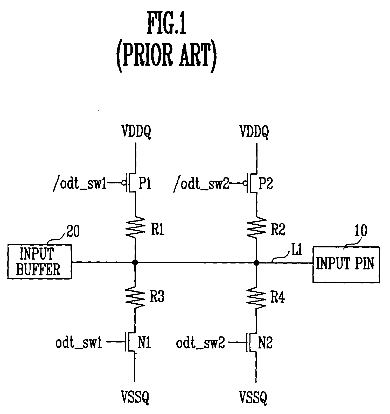
[0016]An on die termination circuit in accordance with a preferred embodiment of the present invention will now be described in detail with reference to the accompanying drawings. The embodiment of the present invention can be modified in various forms, which is not intended to be limiting. The embodiment of the present invention is provided to fully explain the present invention to the ordinary people in the art to which the present invention pertains. Wherever possible, the same reference numerals will be used throughout the drawings and the description to refer to the same or like parts.

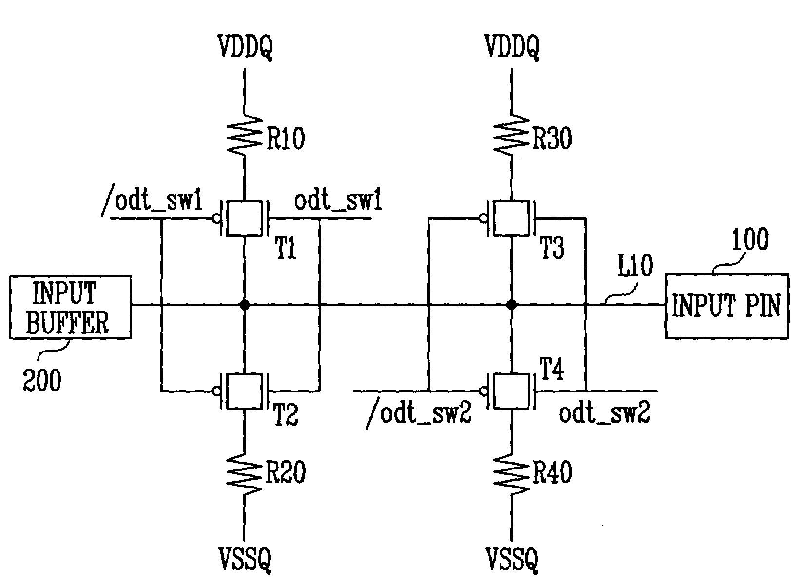
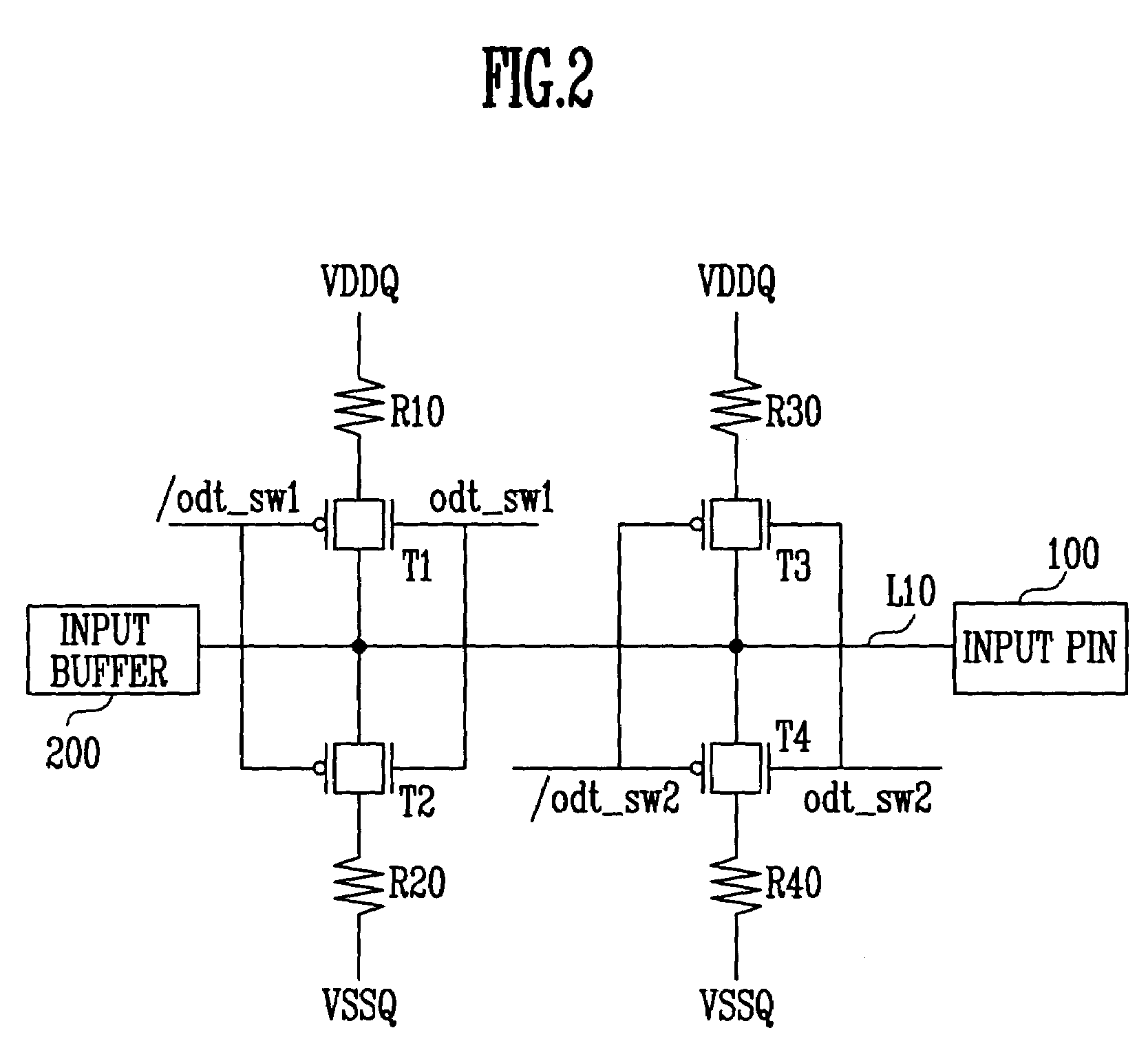
[0017]FIG. 2 is a circuit diagram illustrating the on die termination circuit in accordance with the present invention.

[0018]As illustrated in FIG. 2, the on die termination circuit includes an input transmission line L10 for transmitting a data of an external input pin 100 to an input buffer 200, a first resistor R10 and a first transmission gate T1 driven according to a first termination signal ...


PUM


Abstract

The present invention discloses an on die termination circuit. The on die termination circuit used in a DDR2 employs transmission gates as pull-up and pull-down switches, equalizes pull-up and pull-down resistance values by changing connection relations between switches and resistors, and maintains a constant voltage of an input pin.

Description

BACKGROUND[0001]1. Field of the Invention[0002]The present invention relates to an on die termination circuit, and more particularly to, a switch circuit for turning on or off resistors of an on die termination circuit.[0003]2. Discussion of Related Art[0004]Recently, a memory chip tendency is summarized as high integration and a high data processing speed. A DDR2 popularized in a main memory market is one example showing the tendency. That is, the memory has a capacity over 512 Mb and a data processing speed over 400 Mb per second.[0005]In order to obtain a high data processing speed, the DDR2 newly uses an off chip driver scheme and an on die termination scheme. In the general on die termination scheme, source termination is performed at a transmission side by an output circuit, and parallel termination is performed at a reception side by a termination circuit connected in parallel to a receiving circuit connected to an input pad.[0006]FIG. 1 is a circuit diagram illustrating a co...

Claims


Application Information

Patent Timeline
Patent Type & Authority Patents(United States)
IPC IPC(8): H03K17/16H03K19/094H03K5/12G11C7/10H03K19/003H04L25/02
CPCH04L25/0278A47L9/242
Inventor KWON, DAE HAN
Owner SK HYNIX INC
Why Eureka
Try Eureka