System and method for testing a printed circuit board assembly

a printed circuit board and assembly technology, applied in special-purpose recording/indication devices, instruments, electrophonic musical instruments, etc., can solve the problems of reaching the limits of the industry and no longer being able to guarantee the proper operation of a given design

Active Publication Date: 2007-05-08
NVIDIA CORP
View PDF3 Cites 36 Cited by
  • Summary
  • Abstract
  • Description
  • Claims
  • Application Information

AI Technical Summary

Benefits of technology

[0006]The system and method for testing PCBAs, in accordance with embodiments of the present invention, may be utilized to configure PCBAs to operate using a best set of timing parameters on a per PCBA basis. Embodiments advantageously compensates for manufacturing tolerances and process variations that occur when manufacturing PCBAs.

Problems solved by technology

Due to standard application specific integrated circuit (ASIC) and printed circuit board (PCB) manufacturing tolerances and normal process variations, the industry is reaching the limits where a design using a static qualified setting determined in the product qualification phase is no longer sufficient to guarantee proper operation of a given design across variances in a mass production environment.

Method used


Image

  • System and method for testing a printed circuit board assembly
  • System and method for testing a printed circuit board assembly
  • System and method for testing a printed circuit board assembly

Examples


Embodiment Construction

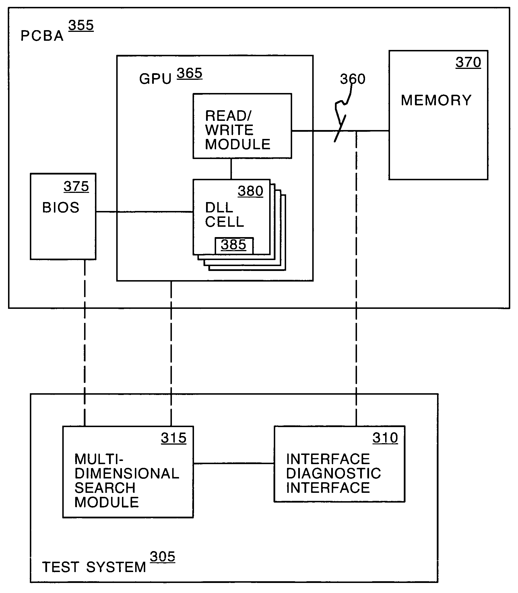
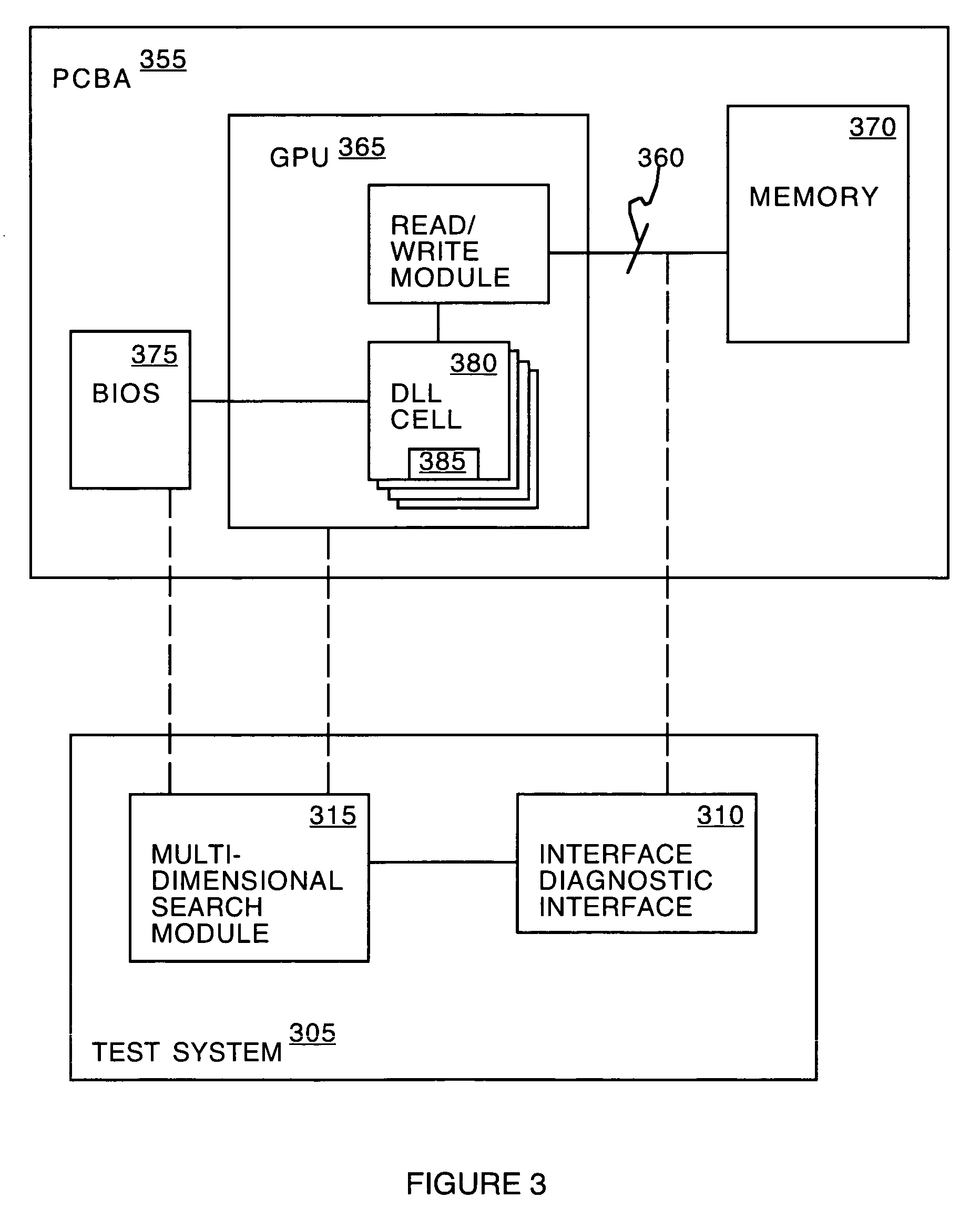
[0013]Reference will now be made in detail to the embodiments of the invention, examples of which are illustrated in the accompanying drawings. While the invention will be described in conjunction with these embodiments, it will be understood that they are not intended to limit the invention to these embodiments. On the contrary, the invention is intended to cover alternatives, modifications and equivalents, which may be included within the scope of the invention as defined by the appended claims. Furthermore, in the following detailed description of the present invention, numerous specific details are set forth in order to provide a thorough understanding of the present invention. However, it is understood that the present invention may be practiced without these specific details. In other instances, well-known methods, procedures, components, and circuits have not been described in detail as not to unnecessarily obscure aspects of the present invention.

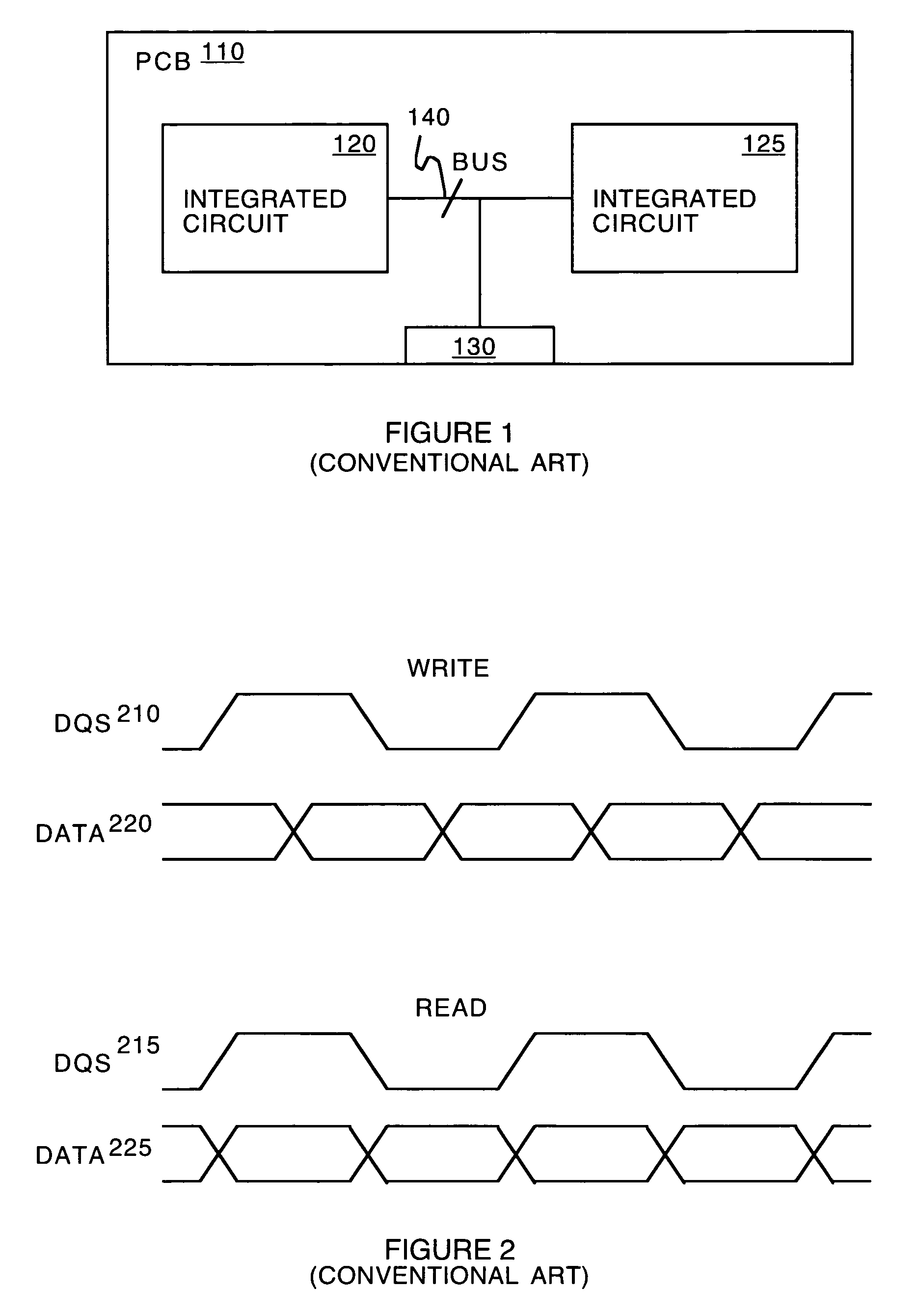
[0014]Referring now to FIG. ...


PUM


Abstract

A system for testing a printed circuit board assembly (PCBA), in accordance with embodiments of the present invention, includes an interface diagnostic module coupled to a multi-dimensional search module. The multi-dimensional search module performs a simultaneous switching output pattern based stress test for each of a plurality of sets of timing parameters. The interface diagnostic module determines an error rate on an interface of the printed circuit board assembly for each of the stress tests. The multi-dimensional search module determines a best set of timing parameters based on the determined error rates.

Description

BACKGROUND OF THE INVENTION[0001]Referring to FIG. 1, a printed circuit board assembly (PCBA), according to the conventional art is shown. As depicted in FIG. 1, the printed circuit board assembly includes a printed circuit board (PCB) 110, integrated circuits (ICs) 120, 125, connectors 130 and the like. The integrated circuits 120, 125 may for example include a central processing unit (CPU), a graphics processing unit (GPU), control circuits, interface circuits (e.g., a north bridge, south bridge or the like), memory and / or the like. The PCB consists of a substrate that has a plurality of traces 140 for interconnecting the ICs 120, 125 and connectors. The traces 140 and the ICs 120, 125 are interconnected to form a given circuit. Typical interconnections (e.g., interface) between one or more ICs and / or a connector include a bus (e.g., system bus, accelerated graphics bus, peripheral component interface, and the like). The bus typically provides for transmission of one or more data ...

Claims


Application Information

Patent Timeline
Patent Type & Authority Patents(United States)
IPC IPC(8): G01D3/00
CPCG01R31/3171G01R31/31725G01R31/318508
Inventor BACHMAN, DAVID A.DAVIES, CARL W.
Owner NVIDIA CORP
Why Eureka
Try Eureka