System and method for debugging system-on-chips

a technology of embedded cores and system-on-chips, applied in error detection/correction, instruments, computing, etc., can solve problems such as problems in the resulting soc, the design techniques used in the design of these socs have not scaled with the complexities of chip design, and the complexity of socs

Inactive Publication Date: 2007-05-15
AVAGO TECH INT SALES PTE LTD
View PDF11 Cites 61 Cited by
  • Summary
  • Abstract
  • Description
  • Claims
  • Application Information

AI Technical Summary

Problems solved by technology

The resulting SoCs have become quite complex.
Moreover, the techniques used in the design of these SoCs have not scaled with the complexities of chip designs.
Frequently, problems in the resulting SoC are encountered in spite of these two levels of testing.
Moreover, if there are problems in a design after the device has been fabricated, it may be extremely difficult to determine the cause of the problems.
This difficulty can be attributed to the number of functional blocks that are potential sources of the problem and the lack of visibility of the internal operation of the SoC device.
In spite of such efforts, functional problems do occur in fabricated devices.
The likelihood of functional problems occurring increases with the complexity of the SoC.
For such complex systems, it is virtually impossible to write vectors to test all the different combinations of functional operation of functional blocks.
Moreover, there may be functional features that the designer did not think about testing.
Further, the functional problem may occur after extended periods of operation and accordingly cannot be easily detected by running simple test vectors.
Often, there is insufficient visibility to the internal state of the SoC device.
As a result, it may take several revisions to the circuit design before the problem is corrected.

Method used


Image

  • System and method for debugging system-on-chips
  • System and method for debugging system-on-chips
  • System and method for debugging system-on-chips

Examples


Embodiment Construction

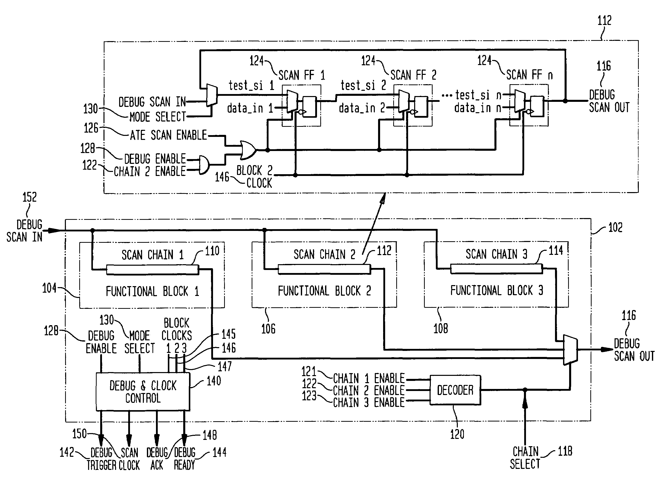
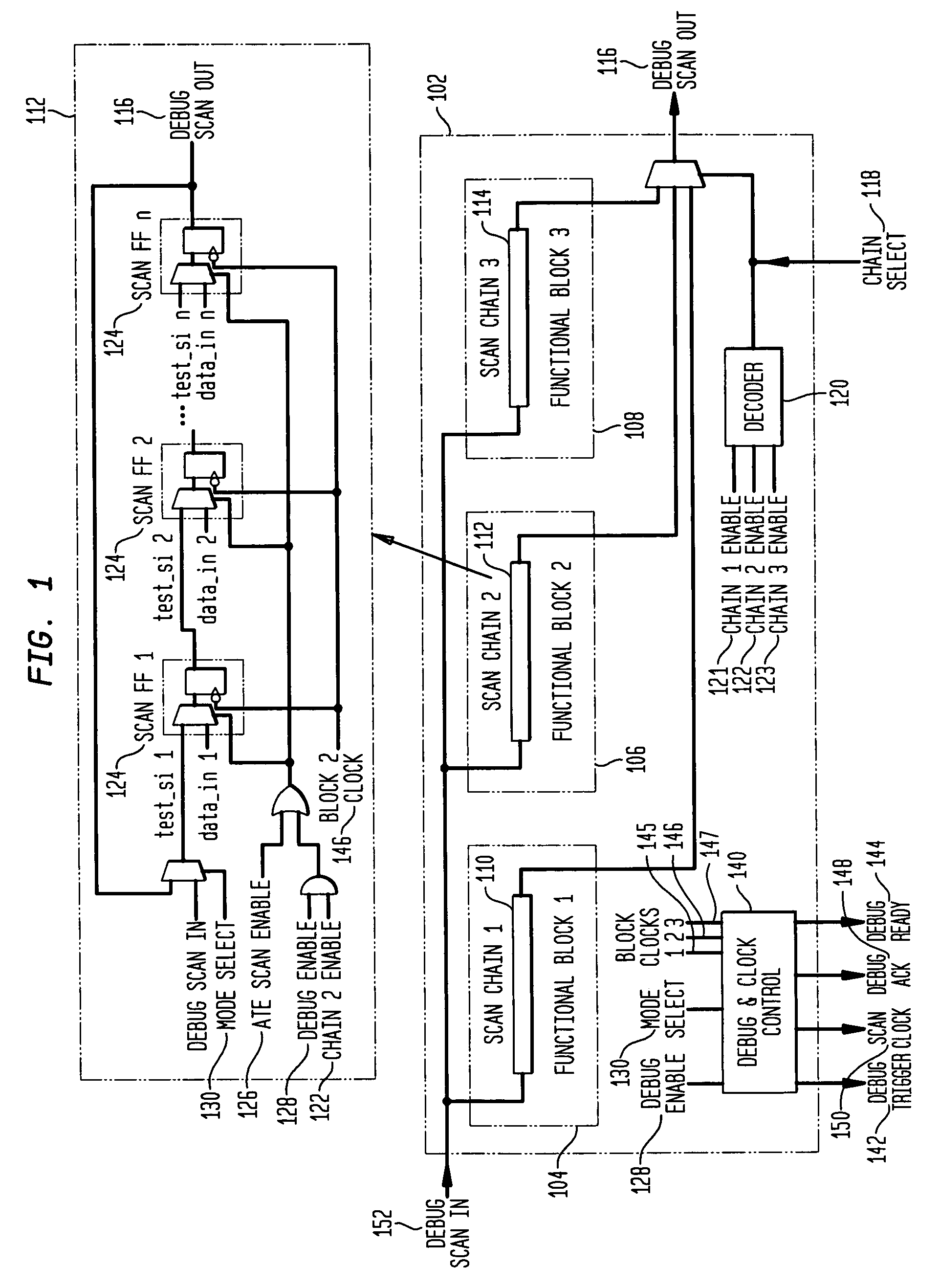
[0014]FIG. 1 illustrates an embodiment of the invention applicable for debugging SoCs. As shown in FIG. 1, SoC 102 includes three functional blocks (functional block 1, functional block 2 and functional block 3; represented by item numbers 104, 106 and 108, respectively). FIG. 1 is intended to be a simple example of an SoC as there frequently are far more functional blocks in an typical SoC. Each functional block may contain one or more scan chains. For simplicity, FIG. 1 shows only one scan chain (item numbers 110, 112 and 114) in each functional block. These scan chains correspond to the chains (or subsets of the chains) used in production testing of the device. By way of example, scan chain 112 is used in the production testing process of functional block 2).

[0015]In the embodiment of the invention illustrated in FIG. 1, outputs from the various scan chains are multiplexed to a single output (debug scan out 116) from which the internal state of the device can be observed. An inpu...


PUM


Abstract

Large, complex SoCs comprise interconnections of various functional blocks. Such functional blocks contain scan chains that are used for their individual production testing. The present invention utilizes these scan chains as a tool in the debugging of these SoCs by providing the internal contents of registers and memories contained on the SoC device. Accordingly, both hardware and software designers are provided a means to observe the effect of their designs on the internal operation of the SoC device. The invention is compatible with current integrated circuit design methodology and requires minimal area on the SoC for support circuitry.

Description

FIELD OF THE INVENTION[0001]The present invention relates to a system and method for debugging embedded cores based system-on-chips (SoCs), and more particularly, to a system and method for debugging complex SoCs by utilizing scan chains contained in individual processor blocks.BACKGROUND OF THE INVENTION[0002]Since the 1990's, integrated circuit (IC) design has evolved from a chip-set philosophy to an embedded core based SoC concept. An SoC IC includes various reusable functional blocks, such as microprocessors, interfaces, memory arrays, and DSPs (digital signal processors). Such pre-designed functional blocks are commonly called “IP cores”, “cores”, or “blocks”, and will collectively be referred to hereafter as “functional blocks” or simply, “blocks”. The resulting SoCs have become quite complex. Moreover, the techniques used in the design of these SoCs have not scaled with the complexities of chip designs. That is, SoCs are currently designed by combining functional blocks from ...

Claims


Application Information

Patent Timeline
Patent Type & Authority Patents(United States)
IPC IPC(8): G06F11/00G06F11/267
CPCG06F11/267
Inventor YEE, OCEAGER P.
Owner AVAGO TECH INT SALES PTE LTD
Why Eureka
Try Eureka