Semiconductor integrated circuit with memory redundancy circuit

a technology of integrated circuits and memory redundancy, which is applied in the direction of instruments, coding, code conversion, etc., can solve the problems of deterioration of soft error immunity, cell size, and inability to read, correct, and output data in a single cycl

Active Publication Date: 2007-05-15
RENESAS ELECTRONICS CORP
View PDF6 Cites 8 Cited by
  • Summary
  • Abstract
  • Description
  • Claims
  • Application Information

AI Technical Summary

Benefits of technology

The present invention is about a semiconductor device with a plurality of memory cells and an error correction circuit. The device allows for both reading and writing to be completed in a single cycle. The memory cells are organized in a way that cells on a specific word line are allocated to different addresses. The device also includes a latch type sense amplifier that supports both a page mode and burst mode for data storage. This allows for efficient error repair in the event of errors. In the writing operation, only data that is different from the previously read data is written. Overall, this invention provides a more efficient and effective semiconductor device for data storage and retrieval.

Problems solved by technology

The technical problem addressed in this patent relates to improving the ability of memory devices to resist damage from radiation or other factors that can cause temporary changes in their behavior. This issue arises because reducing the power supply and making smaller components leads to weaker resistance to these types of events. While some solutions involve applying error correction codes after each access, they often require multiple cycles for recovery and may result in lost data if repeated corrections are needed.

Method used


Image

  • Semiconductor integrated circuit with memory redundancy circuit
  • Semiconductor integrated circuit with memory redundancy circuit
  • Semiconductor integrated circuit with memory redundancy circuit

Examples


first exemplary embodiment

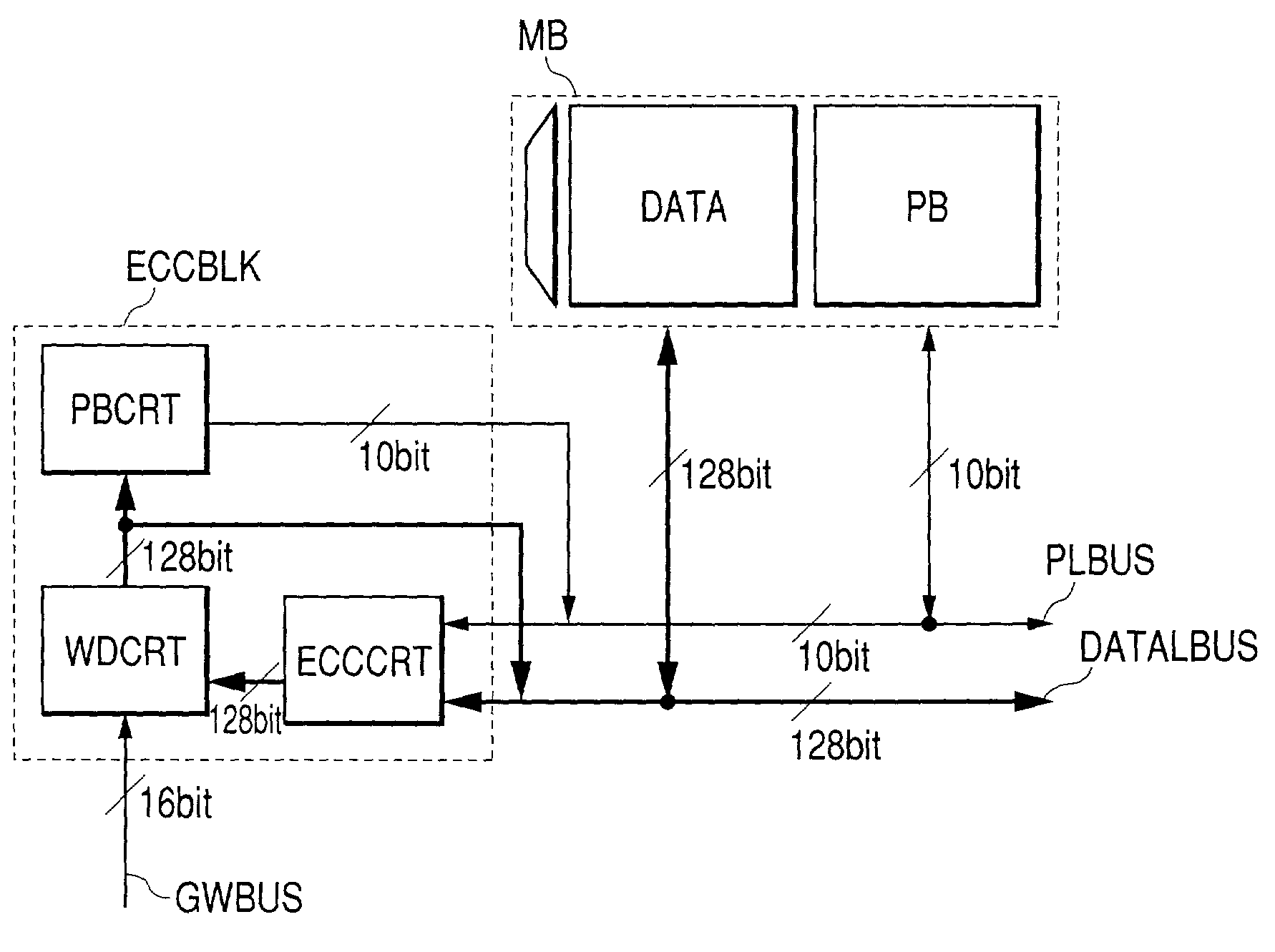
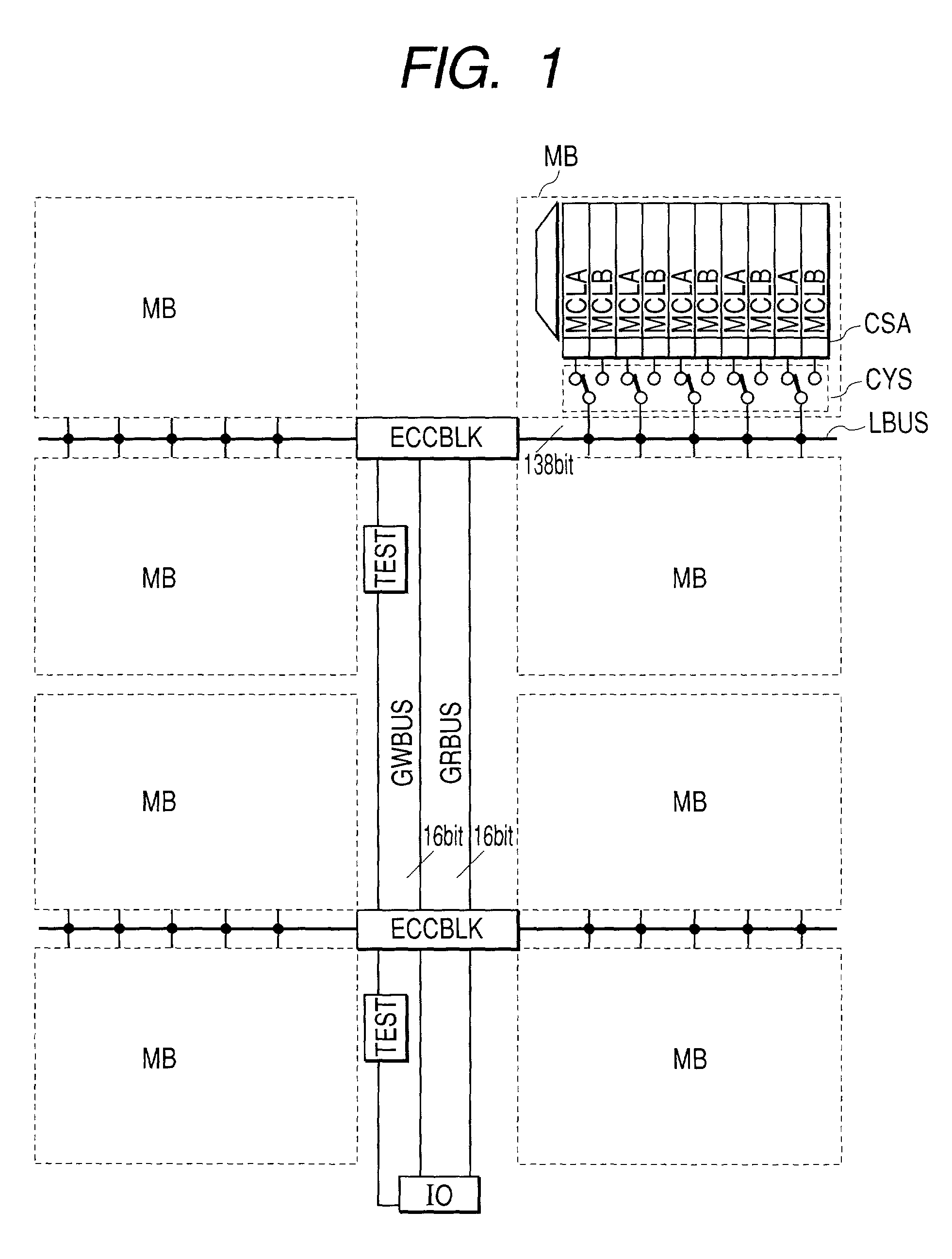
[0020]FIG. 1 is a circuit diagram illustrating an example of an application of the present invention to an SRAM. An SRAM memory with an ECC as a semiconductor memory device is divided into a plurality (eight, in this example) of memory blocks. Each block comprises a memory array, a latch type sense amplifier circuit CSA, and a Y switch circuit CYS. The memory array is comprised of memory columns A (MCLA) and memory columns B (MCLB). The memory columns A and B are allocated to different addresses. For example, assuming that there is one parity bit in every 10-bit address and adjacent memory cells on a word line are allocated to an address, if one of the neighboring memory cells, which share the allocated parity bit, has an error, the error cannot be repaired. On the other hand, if adjacent memory cells are allocated to different addresses, each having its own parity bit, then even if one of the adjacent memory cells has an error, the error can be repaired. Since a soft error is likel...

second exemplary embodiment

[0029]FIG. 3 is a circuit diagram illustrating an example of application of the present invention to an SRAM. This semiconductor memory device is formed on a semiconductor substrate made of a material such as single crystal silicon. An SRAM memory with ECC 200, as a semiconductor memory device, is divided into a plurality (32, in this example) of memory mats MAT. Each memory mat (MAT) comprises a circuit 110 as shown in FIG. 4. Eight memory mats comprise a single memory block (BLOCK); there is a local bus LBUS in the center of the block. In this embodiment, the bus width of the local bus LBUS is 138 bits. An error correction block 145 is provided at the point where the local buses (LBUS0, LBUS1) of two blocks (BLOCK0, BLOCK1) intersect. Likewise, an error correction block 153 is provided at the point where the local buses (LBUS2, LBUS3) of two blocks (BLOCK2, BLOCK3) intersect. The error correction block 145 and the error correction block 153 are interconnected by a global bus for r...

third exemplary embodiment

[0054]The memory mat MAT with a shift type error repair circuit as illustrated by the second exemplary embodiment may be replaced by a circuit 210 with a redundancy circuit for a current defect as shown in FIGS. 7 and 8. FIGS. 7 and 8 make up a diagram with line AA′ as the boundary.

[0055]Referring to FIGS. 7 and 8, the mat circuit 210 will be explained next. The mat (MAT) is comprised of an array block as an arrangement of a plurality of base sets SET, a control circuit 212, and a decoder circuit 213 which specifies a redundancy set.

[0056]A base set SET is comprised of a plurality of units (four units in this embodiment, UNIT0, UNIT1, UNIT2, UNIT3) and a control circuit SETCNT. Each unit is comprised of a plurality of columns of memory cell array (two columns in this embodiment), a circuit 211 for supplying voltage to the memory cell, equalizer precharge circuits (CEQ0, CEQ1), column switches (CRYS0, CRYS1), a sense amplifier CSA, and a write amplifier CWA. Data lines (DT0, DB0) are...


PUM


Abstract

A semiconductor integrated circuit with memory redundancy circuit to address the problems of increased area, power consumption and access time which is caused by using an ECC circuit for error correction. The circuit comprises: a plurality of memory mats; a local bus, parallel to word lines, which transfers read data and write data from memory cells; a global bus for writing, parallel to data lines, which transfers write data from an input pad IO; a global bus for reading, parallel to data lines, which transfers read data to an output pad IO; and at least one error correction circuit located at an intersection of the global buses and the local bus. Reading and writing may each be completed in a single cycle, and during a write operation, data which is different from data previously read is written. By this configuration, an increase in area and power consumption can be avoided and errors such as soft errors can be corrected.

Description


Claims


Application Information

Patent Timeline
Owner RENESAS ELECTRONICS CORP
Why Eureka
Try Eureka