Light emitting device and method for fabricating light emitting device

a light emitting device and light emitting device technology, applied in the direction of instruments, discharge tube luminescnet screens, non-linear optics, etc., to achieve the effect of suppressing the potential drop of a counter electrode, high precision and precise pattern

Active Publication Date: 2007-05-22
SEMICON ENERGY LAB CO LTD
View PDF43 Cites 70 Cited by
  • Summary
  • Abstract
  • Description
  • Claims
  • Application Information

AI Technical Summary

Benefits of technology

[0009]In view of the above problem, it is an object of the present invention to provide a method for fabricating a light emitting device, in which brightness gradient due to potential drop of a counter electrode can be prevented from being observed and an auxiliary electrode can be formed without increasing the number of steps, even when the precision of a light emitting device is improved. It is another object of the invention to provide a light emitting device fabricated according to the method.
[0011]The auxiliary electrode can suppress the potential drop of a counter electrode and prevent brightness gradient from being observed in a pixel area. The invention is particularly effective in a light emitting device of the top emission type whose auxiliary electrode is difficult to be formed all over the counter electrode.
[0013]The method for connecting an auxiliary electrode and a counter electrode according to the invention is not limited to the method using the step coverage. Alternatively, when a light emitting layer is formed by vapor deposition using a metal mask, it is another option to form an area where the light emitting layer is not formed and to electrically connect the auxiliary electrode to the counter electrode. In the case of a full color display light emitting device which is fabricated by separately applying light emitting layers corresponding to each color of the three primary colors using a metal mask, the area where a light emitting layer is not formed can be formed by using the metal mask; thus, the contact can be made by employing the above method without increasing the number of steps.
[0016]According to the invention, an auxiliary electrode can be formed by using a photolithography since the auxiliary electrode is formed before forming a light emitting element. Further, a precise pattern can be formed by using the photolithography. Accordingly, even if the width between light emitting elements is reduced to less than 20 μm due to the high precision, the auxiliary electrode can be formed to fit within the width. Further, according to the invention, the auxiliary electrode is formed by photolithography as the same as wirings of a pixel area, a gate electrode, and the like that are formed from a conductive film; thus, the auxiliary electrode can be formed without increasing the number of steps. The auxiliary electrode can suppress the potential drop of a counter electrode and prevent brightness gradient from being observed in a pixel area. The invention is particularly effective in a light emitting device of the top emission type whose auxiliary electrode is difficult to be formed all over the counter electrode.

Problems solved by technology

Namely, an auxiliary electrode and a counter electrode are electrically connected in an area which is not covered with the light emitting layer due to the inferiority in step coverage.

Method used


Image

  • Light emitting device and method for fabricating light emitting device
  • Light emitting device and method for fabricating light emitting device
  • Light emitting device and method for fabricating light emitting device

Examples


embodiment mode 1

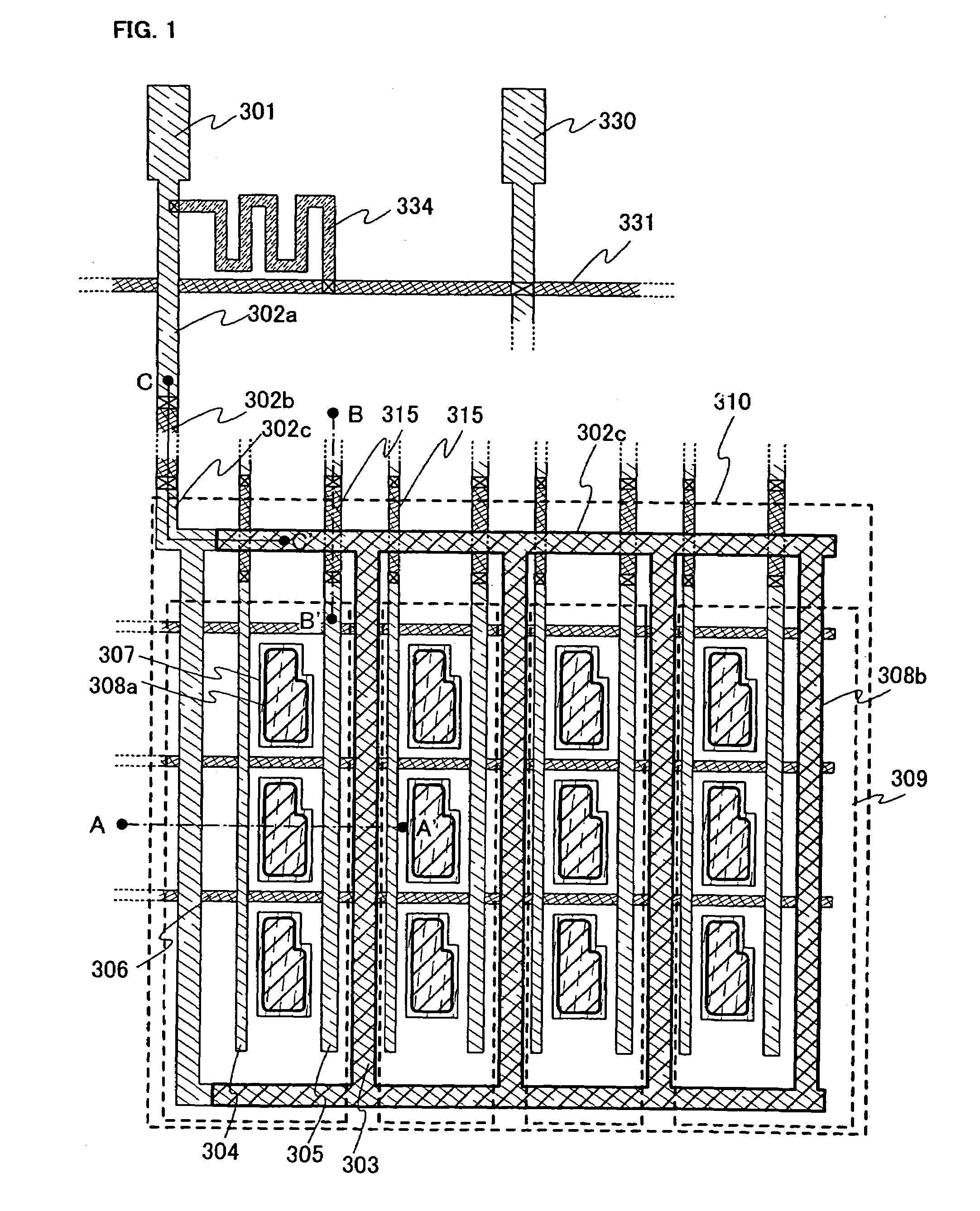
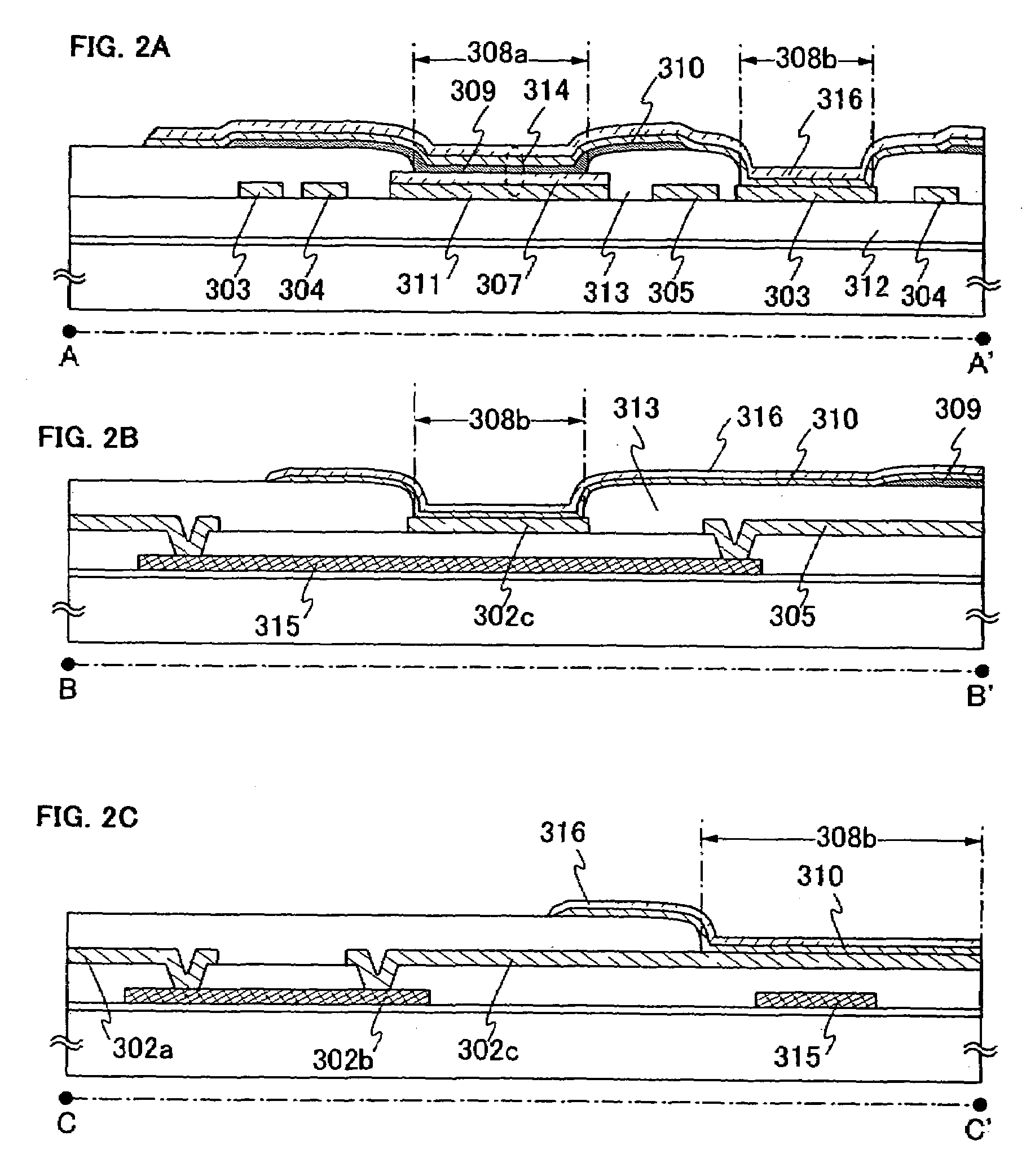
[0044]The configuration of a pixel area in a light emitting device of this embodiment mode will be described with reference to FIG. 1. FIG. 1 shows a top view of a pixel area and a leader wiring. Reference numeral 301 denotes a connection terminal, and reference numerals 302a, 302b, and 302c denote leader wirings. Further, an electrode 303 formed in the pixel area is equivalent to an auxiliary electrode, and the electrode is connected to the connection terminal 301 via the leader wirings 302a, 302b, and 302c. In FIG. 1, the connection terminal 301 and the auxiliary electrode 303 are electrically connected by using the three leader wirings of 302a, 302b, and 302c. However, the configuration of leader wirings is not limited to the configuration shown in FIG. 1, and any configuration may be used as long as the connection terminal 301 and the auxiliary electrode 303 can be connected electrically. All of a connection terminal, a leader wiring, and an auxiliary electrode may be formed fro...

embodiment mode 2

[0060]In this embodiment mode, a mode of a shape of an opening, which is different from the one in Embodiment Mode 1 will be described.

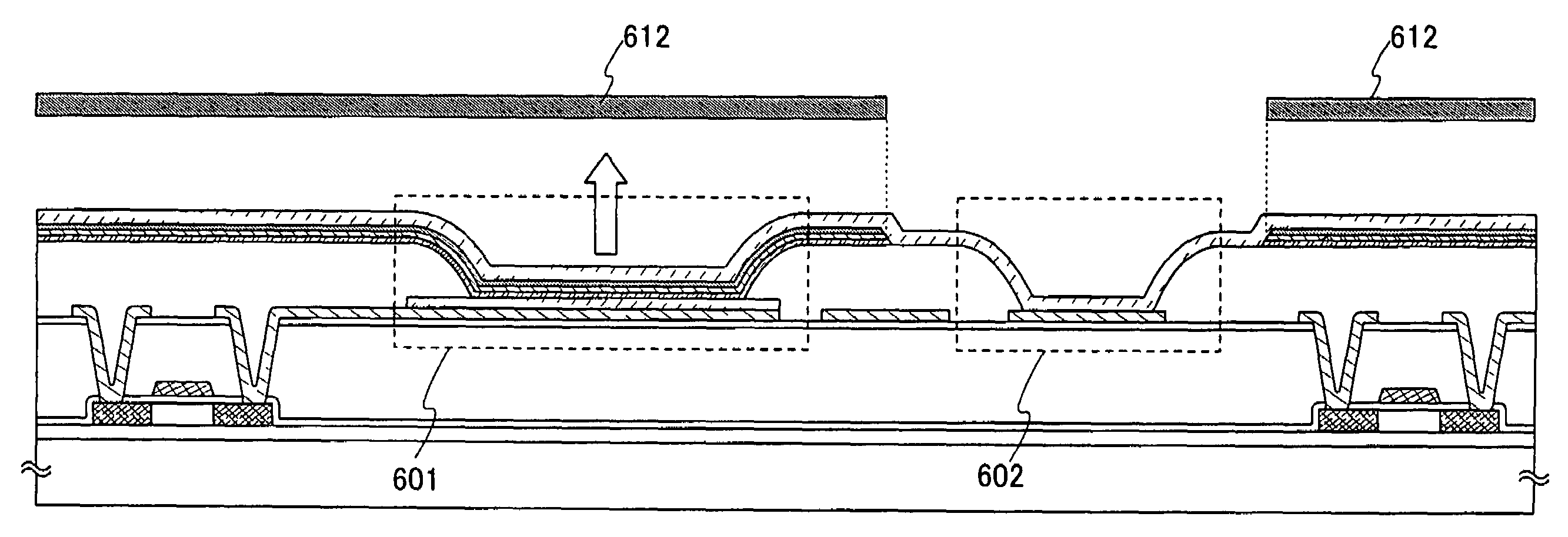
[0061]FIG. 3 shows a top view of a pixel area in this embodiment mode. Reference numeral 403 denotes an opening, and a counter electrode 404 and an auxiliary electrode 401 are electrically connected in an opening 403. In this embodiment mode, when an electroluminescent layer 405 is formed so as not to entirely cover the opening 403 by using a metal mask; thus, the auxiliary electrode 401 is connected to the counter electrode 404 directly or electrically in the opening 403. In this case, the end portion of the auxiliary electrode may be exposed in the opening, or may be covered with a second interlayer insulating film.

[0062]The end portion of the auxiliary electrode 401 may be exposed in the opening 403, and a part which is not covered by the electroluminescent layer 405 may be deliberately provided in the end portion by means of coverage thereby conn...

embodiment mode 3

[0066]In this embodiment mode, a mode in which a structure of a portion where an auxiliary electrode and a counter electrode are connected is different from that of Embodiment Mode 1 will be described.

[0067]The configuration of a pixel area in a light emitting device of this embodiment mode will be described with reference to FIG. 9. FIG. 9 shows a top view of a pixel area and a leader wiring. Reference numeral 101 denotes a connection terminal, 102a, 102b, 102c denote leader wirings, and 103 denotes an auxiliary electrode. As in FIG. 1, the auxiliary electrode 103 is electrically connected to the connection terminal 101 via leader wirings 102a, 102b, and 102c.

[0068]As in Embodiment Mode 1, a scan line 106, a signal line 104, and a power line 105 are provided in the pixel area. The wirings to be provided in the pixel area of the invention is not limited to the three wirings, and some other wirings than the above wirings may be provided depending on the pixel structure. Further, as ...


PUM


Abstract

It is an object of the present invention to provide a method for fabricating a light emitting device, in which brightness gradient due to potential drop of a counter electrode can be prevented from being observed and an auxiliary electrode can be formed without increasing the number of steps, even when the precision of a light emitting device is improved. It is another object of the invention to provide a light emitting device fabricated according to the method. The light emitting device has a light emitting element and an auxiliary electrode in each pixel. The light emitting element includes a first electrode, a second electrode, an electroluminescent layer provided between the first and the second electrodes. Further, the first electrode is overlapped with the electroluminescent layer and the second electrode formed over an insulating film by means of a first opening formed in the insulating film. Still further, the auxiliary electrode is overlapped with the second electrode by means of a second opening formed over the second insulating film.

Description

BACKGROUND OF THE INVENTION[0001]1. Field of the Invention[0002]The present invention relates to a light emitting device in which a light emitting element and an element for supplying current to the light emitting element are provided for each of a plurality of pixels and to a method for fabricating the light emitting device.[0003]2. Description of the Related Art[0004]A light emitting element has high visibility since it emits light by itself, and is most suitable for thinning since it does not need a backlight, which is required in a liquid crystal display device (LCD); further, there is no limitation of viewing angle either. Therefore, a light emitting device with the use of a light emitting element has been attracting attention as a display device which replaces a CRT and an LCD. In late years, a light emitting device has been put to practical use; for example, it is provided in a cellular phone or an electronic device such as a digital still camera.[0005]A light emitting elemen...

Claims


Application Information

Patent Timeline
Patent Type & Authority Patents(United States)
IPC IPC(8): H01J1/62H01J63/04H01L27/32H01L51/50H01L51/52H05B33/00H05B44/00
CPCH01L27/3276H01L51/5221H01L27/3246H01L27/3248H01L2251/5315H01L51/5203H01L51/5092G02F1/136204H10K59/122H10K59/123H10K59/1315H10K50/171H10K50/824H10K50/828H10K2102/3026H10K59/805H10K50/805
Inventor YAMAZAKI, SHUNPEINAGAO, RITSUKONAKAMURA, YASUO
Owner SEMICON ENERGY LAB CO LTD
Why Eureka
Try Eureka