Semiconductor memory device and manufacturing method thereof

a memory device and semiconductor technology, applied in the direction of semiconductor devices, electrical devices, transistors, etc., can solve the problems of large number of steps in the manufacturing method, insufficient reduction of cell size attained, and large cell area tend to become considerably large, so as to improve the -ray soft error resistance of the sram and facilitate the reduction of memory cell size

Inactive Publication Date: 2005-10-13
RENESAS ELECTRONICS CORP
View PDF5 Cites 1 Cited by
  • Summary
  • Abstract
  • Description
  • Claims
  • Application Information

AI Technical Summary

Benefits of technology

[0016] The present invention can provide a SRAM whose memory cell size is readily reduced without unduly increasing the number of the steps in the manufacturing method thereof. Further, the present invention can improve the α-ray soft error resistance of the SRAM.
[0094] In the present invention, by forming a pair of local interconnections from different conductive layers, it becomes possible to dispose these two local interconnections partially overlapped with each other so that the occupied area of the memory cell can be well reduced.
[0095] Further, in the present invention, because a pair of the local interconnections separated by an insulating film can constitute a capacitor element, α-ray soft error resistance can be prevented from lowering, which may take place along with miniaturization of the memory cell size or a decrease in operation voltage.
[0096] Further, in the present invention, when one of the local interconnections set in a lower layer is made of an inlaid interconnection, formation of this lower layer local interconnection can be made, together with formation of a contact plug so that fabrication thereof can be achieved with the small number of steps. Further, when one of the local interconnection set in a lower layer is made of an inlaid interconnection, due to improved planarity, it becomes possible, with ease, to form thinly as well as uniformly a capacitor insulating film and the other one of local interconnections which are set in an upper layer, which may improve the yield and element characteristics.
[0097] Further, in the present invention, through formation of a refractory metal silicide layer that is a low-resistance material on source / drain regions or gate electrodes, a still higher speed operation can be attained without relying upon a symmetry of the SRAM structure.

Problems solved by technology

However, the SRAM cell described above has a problem that a cell area tends to become considerably large, due to requirements to have 6 transistors in one memory cell and isolate p-type MOSs from n-type MOSs within one and the same cell as well as the need of numerous interconnections.
Another disadvantage it has is the large number of the steps in the manufacturing method thereof.
Nevertheless, in this method, because the other one (an upper layer) of the local interconnections should be formed in such a way that its disposition could avoid any contact with the lower layer of the local interconnections, a reduction in cell size attained cannot be sufficiently large.
Yet, in this method, too, it is difficult to achieve a sufficient reduction in cell size, since a pair of local interconnections must be disposed so as not to come into contact with each other.
However, for such an element structure, a contact hole must be formed separately for each one of a pair of local interconnections so that a substantially large number of steps are required in its fabrication.
When a conductive film pattern is to be formed on such an uneven substrate surface, there arises a problem that superfluous parts of the conductive film may remain at unrequired positions because, in performing patterning of the conductive film by means of anisotropic etching, it is difficult to remove portions of the conductive film around stepped parts.
On the other hand, if the film thickness around the stepped parts is to be made satisfactorily thin, there may arise another problem that the film thickness in the flat region becomes excessively thin, which may result in damage to insulation thereof.
In short, formation of a thin and, at the same time, even capacitor insulating film is difficult to achieve.

Method used


Image

  • Semiconductor memory device and manufacturing method thereof
  • Semiconductor memory device and manufacturing method thereof
  • Semiconductor memory device and manufacturing method thereof

Examples


first and second embodiments

[0142] Next, First and Second Embodiments of the present invention are described below.

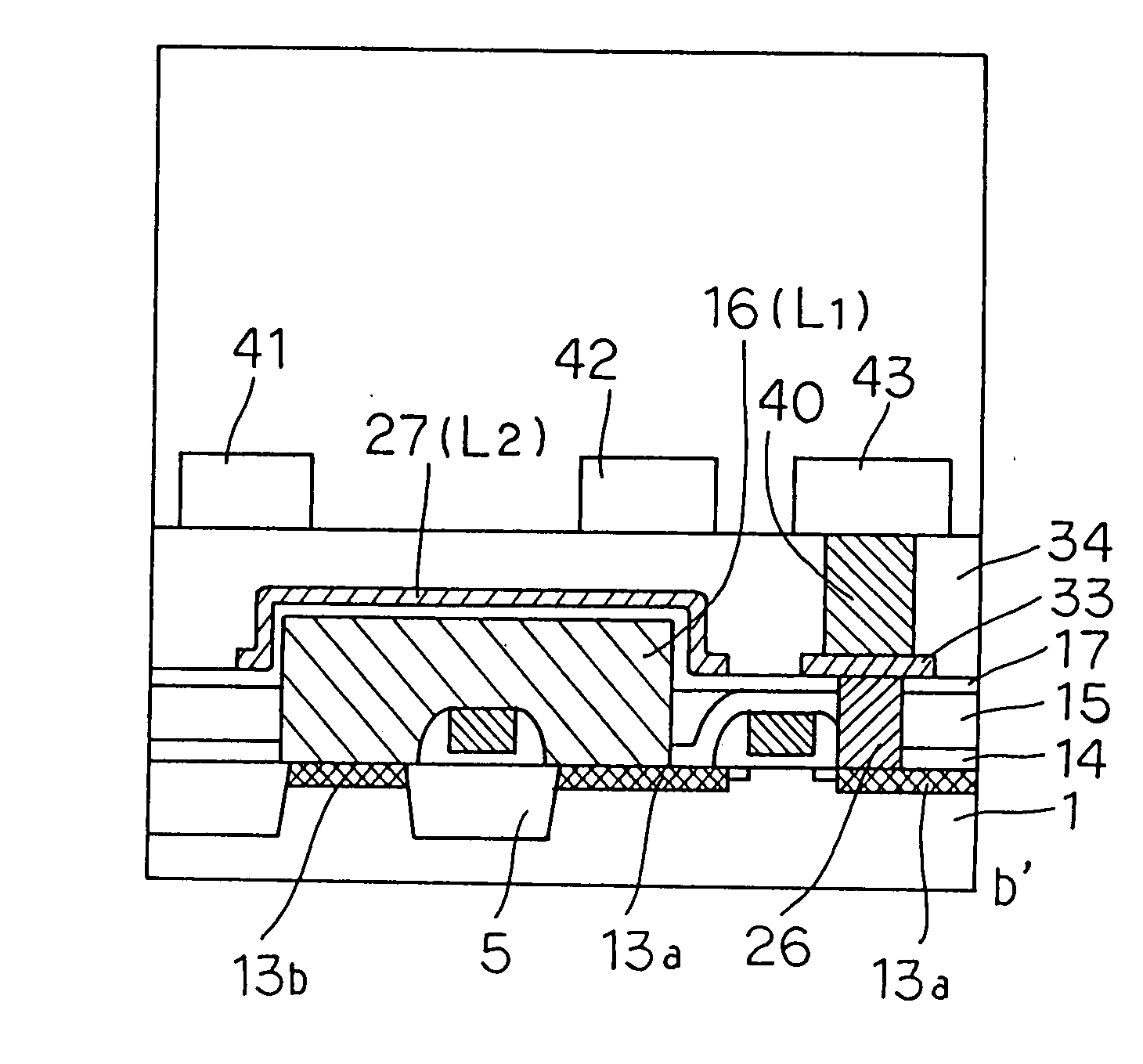
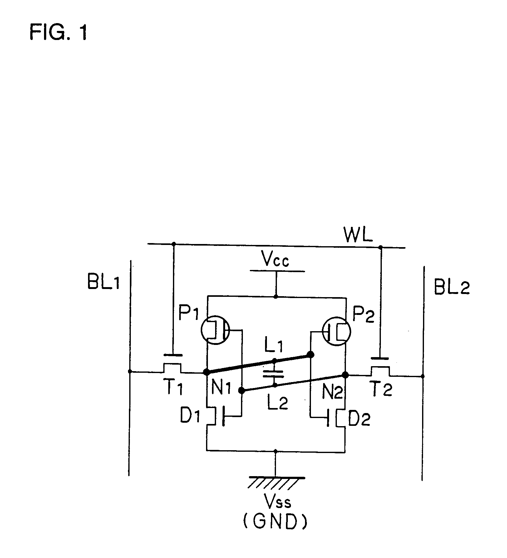
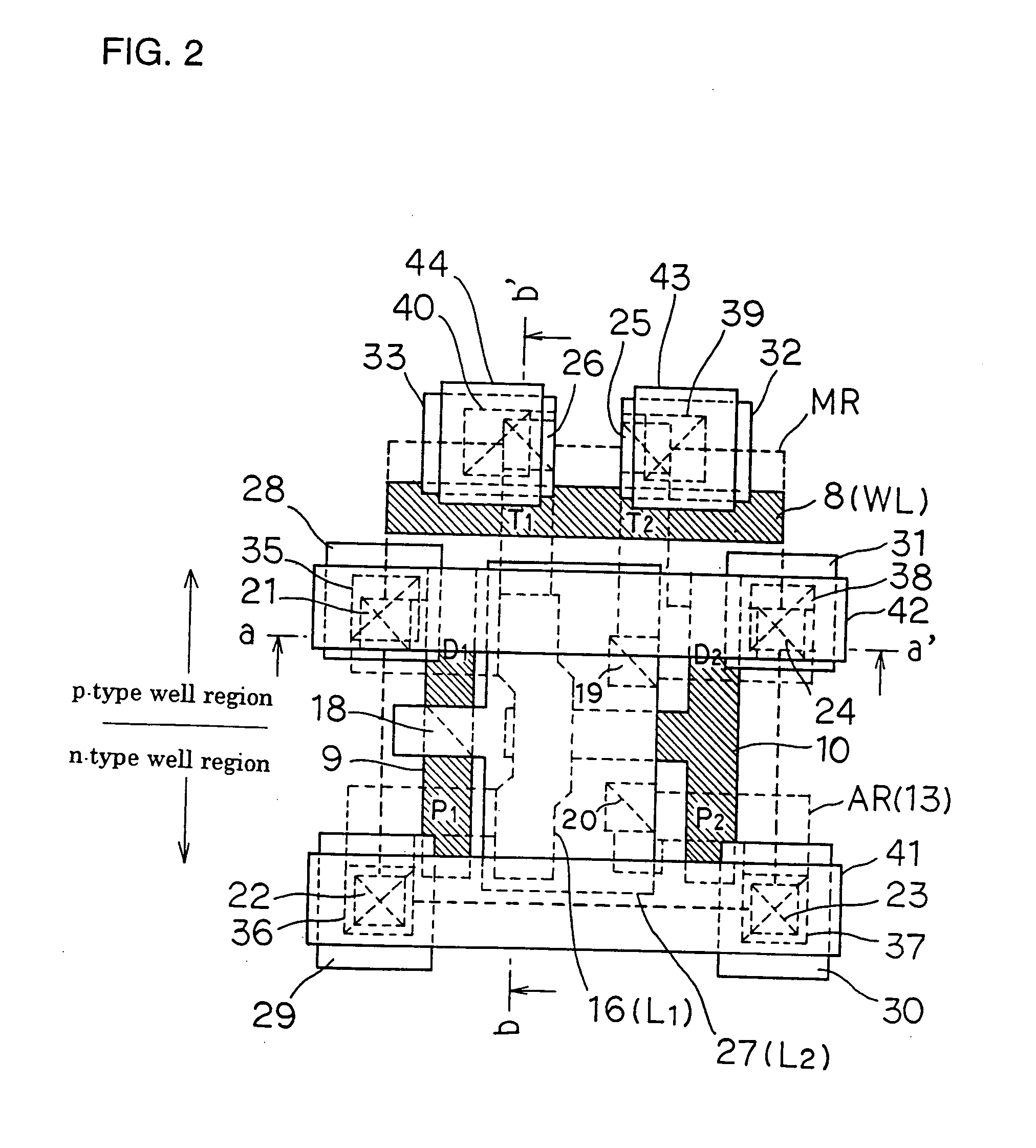
[0143] In the First Embodiment, a pair of local interconnections L1 and L2 are disposed in two different layers, with the local interconnection in a lower layer being formed of an inlaid (damascene) interconnection and the local interconnection in an upper layer, formed of a conductive film in the form of a plate. Further, the disposition of these local interconnection is arranged in such a way that, seen from the top surface (the top surface plane) of the substrate, a portion of the upper layer local interconnection (the plate-shaped interconnection) overlaps at least a portion of the top surface of the lower layer local interconnection (the inlaid interconnection), with an insulating film lying therebetween. Herein, the lower layer local interconnection (the inlaid interconnection) and the upper layer local interconnection (the plate-shaped interconnection), separated by an insulating film, con...

third embodiment

[0185] A cross-sectional view showing a structure of the present embodiment is presented in FIG. 23. FIGS. 23 (a) and (b) corresponds to FIGS. 3(a) and (b) showing a structure of the First Embodiment, respectively.

[0186] In the structure of the present embodiment, a stacked electrode 101 is disposed on a lower layer local interconnection 16 (L1) that is an inlaid interconnection. A plate-shaped upper layer local interconnection 27 (L2) is disposed so as to cover, at least, a portion of the top surface as well as a portion of the lateral face of this stacked electrode 101 with an insulating film 17 lying therebetween. Although, in the drawing, the top surface and the lateral face of the stacked electrode 101 are partially covered, both of the faces can be entirely covered, as far as the margin permits. In such a structure, a capacitor element is formed also on the lateral face of the stacked electrode so that the capacitance of the element can be significantly raised.

[0187] The str...

fourth embodiment

[0189] A cross-sectional view showing a structure of the present embodiment is presented in FIG. 27. FIGS. 27 (a) and (b) corresponds to FIGS. 3(a) and (b) showing a structure of the First Embodiment, respectively.

[0190] In the structure of the present embodiment, a trench is set in a third interlayer insulating film 34 which is set, prior to an application of a second interlayer insulating film 17 that is to serve as a capacitor insulating film, and in this trench, there is formed a capacitor element composed of a cylinder electrode (an electrode film in trench, taking the shape of a hollow prism) 111 which covers the inside sidewall of the trench and besides the bottom of which comes into contact with the lower layer local interconnection 16 (L1) and a buried electrode 112 which fills up the trench after a second interlayer insulating film 17 is applied thereto, and the second interlayer insulating film 17 placed therebetween. In such a structure, a capacitor element is formed al...


PUM


Abstract

The present invention relates to a semiconductor memory device having a SRAM in which a memory cell comprises a pair of transmission transistors and a flip-flop circuit containing a pair of driver transistors and a pair of load transistors, wherein: a first conductive film interconnection formed from a first conductive film which is set on a semiconductor substrate, constitutes respective gate electrodes of said driver transistors, load transistors and transmission transistors; an inlaid interconnection set in a first insulating film lying on said semiconductor substrate, constitutes one of a pair of local interconnections cross-coupling a pair of input / output terminals in said flip-flop circuit; and a second conductive film interconnection formed from a second conductive film which is set on a second insulating film lying on said first insulating film, constitutes the other one of said pair of local interconnections. The present invention can provide a SRAM whose memory cell size is readily reduced without unduly increasing the number of the steps in the manufacturing method thereof. Further, the present invention can improve the α-ray soft error resistance of the SRAM.

Description

TECHNICAL FIELD [0001] The present invention relates to a semiconductor memory device and a manufacturing method thereof and more particularly to a semiconductor memory device having a SRAM (Static Random Access Memory) and a manufacturing method thereof. BACKGROUND OF THE INVENTION [0002] With reference to a drawing, the basic structure of a SRAM memory cell that is a semiconductor memory element is described below. [0003] As shown in a circuit diagram of FIG. 22, a SRAM memory cell is composed of a flip-flop circuit that functions as an information storage section and a pair of transmission transistors T1 and T2 that control the conduction between data lines (bit lines, BL1 and BL2) which serve for writing and reading of the information and the flip-flop circuit. The flip-flop circuit is made of, for example, a pair of CMOS (Complementary Metal Oxide Semiconductor) inverters and each CMOS inverter contains a driver transistor D1 (D2) and a load transistor P1 (P2). [0004] One side ...

Claims


Application Information

Patent Timeline
Patent Type & Authority Applications(United States)
IPC IPC(8): H01L31/062H01L21/8244H01L27/11
CPCH01L27/11H01L27/1104H10B10/00H10B10/12H10B99/00
Inventor NATSUME, HIDETAKA
Owner RENESAS ELECTRONICS CORP
Why Eureka
Try Eureka