Semiconductor device and method of manufacturing the same

a technology of semiconductors and semiconductors, applied in semiconductor devices, electrical devices, transistors, etc., can solve the problems of complex process flow, increased short channel effect, excessive widened depletion layer, etc., to achieve the effect of suppressing high withstanding voltage mosfet, increasing the number of steps, and maintaining cost and manufacturing tim

Active Publication Date: 2012-08-07
ABLIC INC
View PDF4 Cites 0 Cited by
  • Summary
  • Abstract
  • Description
  • Claims
  • Application Information

AI Technical Summary

Benefits of technology

[0009]It is an object of the present invention to provide a method of manufacturing a high withstanding voltage metal oxide semiconductor field effect transistor (MOSFET) in which a short channel effect is suppressed, which is capable of maintaining cost and manufacturing time of the conventional high withstanding voltage MOSFET without making complex a process flow and increasing the number of steps of a conventional high withstanding voltage MOSFET.
[0010]According to the present invention, in order to achieve the above-mentioned object, the following method is employed. In a channel forming region, a region to be doped with impurities and a region to be doped with no impurity are provided when ion implantation of the impurities is performed in the channel forming region, for controlling a threshold voltage. The region to be doped with no impurity is suitably patterned so that impurity concentration of the channel forming region near boundaries between a well region and a low concentration source region and between the well region and a low concentration drain region, which has the same conductivity type as that of the well region, may be increased, to thereby induce a reverse short channel effect. By canceling the short channel effect with the reverse short channel effect induced by the above-mentioned method, the short channel effect of the high withstanding voltage MOSFET may be suppressed.
[0011]According to the present invention, the region to be doped with the impurities and the region to be doped with no impurity are suitably patterned when impurity ions are implanted into the channel forming region, for controlling the threshold voltage. As a result, without making complex the process flow and increasing the number of steps, the short channel effect of the high withstanding voltage MOSFET may be suppressed.

Problems solved by technology

However, the low impurity concentrations of the low concentration source region 3 and the low concentration drain region 4 induce reduction in impurity concentrations of the low concentration source region 3 and the low concentration drain region 4 in boundary portions with the adjacent p-type well region 2, with the result that a depletion layer is excessively widened, and hence there is a problem that a short channel effect is increased.
However, the process flow becomes complicated and the number of steps increases compared to a manufacturing method for a conventional high withstanding voltage MOSFET, and hence there is a disadvantage in view of cost and manufacturing time since a groove-like trench needs to be formed between the source region and the drain region in the trench gate type high withstanding voltage MOSFET according to JP 2008-166717 A.

Method used


Image

  • Semiconductor device and method of manufacturing the same
  • Semiconductor device and method of manufacturing the same
  • Semiconductor device and method of manufacturing the same

Examples


Embodiment Construction

[0021]Hereinafter, an embodiment according to the present invention is described in detail.

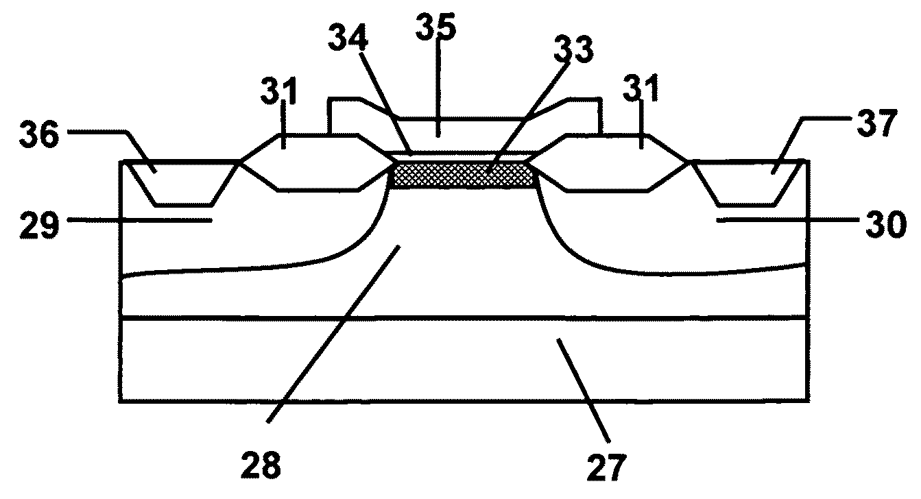
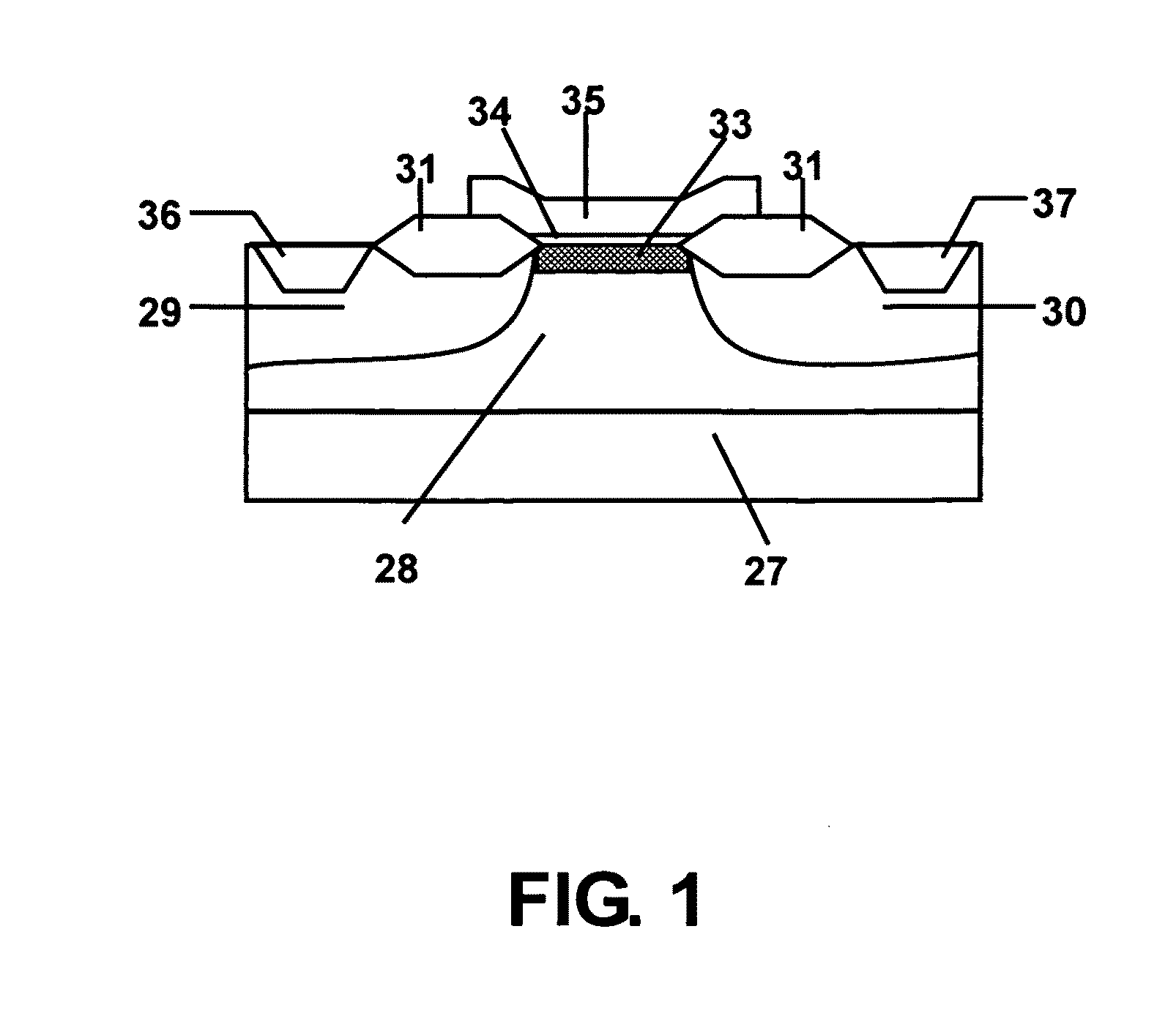
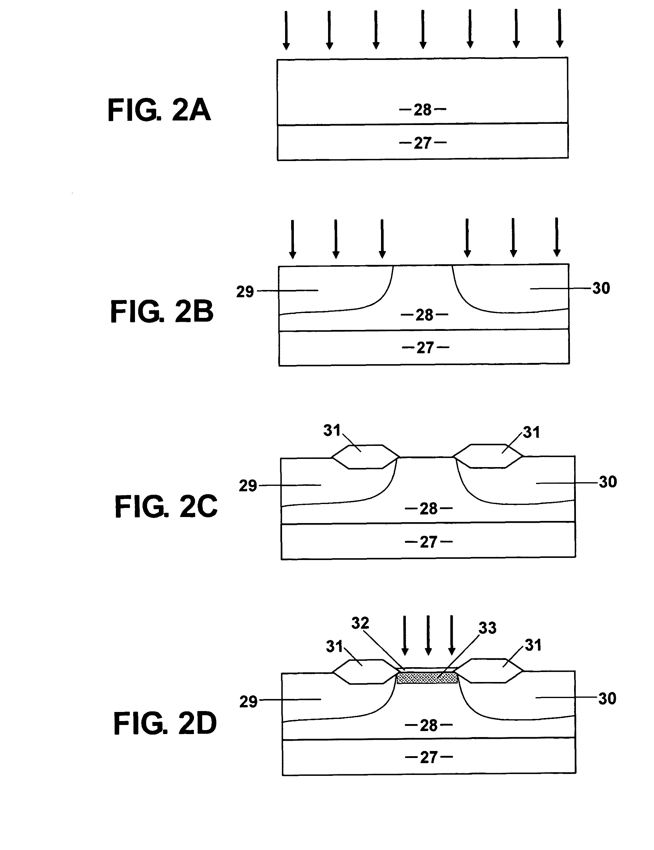
[0022]FIG. 1 is a cross-sectional view illustrating an element structure of a high withstanding voltage metal oxide semiconductor field effect transistor (MOSFET) according to the present invention. A well region 28 of a first conductivity type is formed along a main surface of a semiconductor substrate 27. The well region 28 is doped with low concentration impurities of a second conductivity type so that a low concentration source region 29 and a low concentration drain region 30 are formed as being spaced apart from each other. Further, the low concentration source region 29 and the low concentration drain region 30 are doped with high concentration impurities of a second conductivity type so that a high concentration source region 36 and a high concentration drain region 37 are formed therein, respectively.

[0023]A first and second field insulating films 31 are formed so as to be spaced apar...


PUM


Abstract

In a method of manufacturing a high withstanding voltage MOSFET, a region to be doped with impurities and a region to be doped with no impurity are provided when ion implantation of the impurities is performed in the channel forming region, for controlling a threshold voltage. The region to be doped with no impurity is suitably patterned so that impurity concentration of the channel forming region near boundaries between a well region and a source region and between the well region and a drain region having the same conductivity type as the well region may be increased, to thereby induce a reverse short channel effect. By canceling a short channel effect with the reverse short channel effect induced by the above-mentioned method, the short channel effect of the high withstanding voltage MOSFET may be suppressed.

Description

BACKGROUND OF THE INVENTION[0001]1. Field of the Invention[0002]The present invention relates to a semiconductor device including a high withstanding voltage metal oxide semiconductor field effect transistor (MOSFET) and a method of manufacturing the same.[0003]2. Description of the Related Art[0004]Conventionally, various efforts have been made so as to attain high withstanding voltage of a MOSFET. As one example of the efforts, there has been proposed a method of diffusing low concentration impurities in a region adjacent to a drain region or in a part of the drain region, so as to reduce an electric field concentration occurring near a surface of the drain region, which is a one of the factors of withstanding voltage deterioration.[0005]A typical structure of the above-mentioned high withstanding voltage MOSFET is described based on an example of an n-channel type MOSFET using a p-type substrate, with reference to a cross-sectional view illustrated in FIG. 6. A p-type well 2 is f...

Claims


Application Information

Patent Timeline
Patent Type & Authority Patents(United States)
IPC IPC(8): H01L29/78H01L21/336
CPCH01L29/0649H01L29/0847H01L29/1045H01L29/105H01L29/66568H01L29/7834
Inventor INOUE, AYAKOSAITOH, NAOTO
Owner ABLIC INC
Why Eureka
Try Eureka