Charge pump DC/DC converter circuit

a converter circuit and dc/dc technology, applied in the direction of dc-dc conversion, power conversion systems, instruments, etc., can solve the problems of extremely large charging current flows, adverse effects on other devices, circuit malfunction, etc., and achieve the effect of restricting the current flowing into the semiconductor switch and increasing the on-resistan

Active Publication Date: 2007-05-29
SHARP KK
View PDF4 Cites 75 Cited by
  • Summary
  • Abstract
  • Description
  • Claims
  • Application Information

AI Technical Summary

Benefits of technology

[0020]According to this arrangement, a potential difference between terminals of one of the first semiconductor switches being turned on in the first period is detected, and a determining signal corresponding to the potential difference is outputted. In accordance with the determining signal, a drive signal is supplied to the semiconductor switches being turned on in the first period. This drive signal increases the on-resistances of these semiconductor switches, in proportion to the detected potential difference.
[0021]As a result, the on-resistances of the semiconductor switches being turned on in the first period increase as the aforesaid potential difference increases, and hence currents flowing into the semiconductor switches are restrained.
[0023]Therefore, the more the rush current and peak current are likely to occur, the more the restraint of such currents is carried out effectively. Moreover, a conventional arrangement of semiconductor switches is usable.

Problems solved by technology

The above-described conventional DC / DC converter circuit is disadvantageous in that a rush current or a peak current flows when the step-up operation is carried out while the capacitors C51 or C52 is not sufficiently charged, thereby exerting an adverse effect on other devices.
As a result, an extremely large charging current flows.
In a case where the aforesaid circuits commonly use the same power source Vin, the voltage Vin may decrease on account of wire resistance influenced by the rush current and peak current, thereby causing malfunction of the circuit.
Furthermore, if a current larger than a permissible amount of the wire flows, the wire for the power source may break down.

Method used


Image

  • Charge pump DC/DC converter circuit
  • Charge pump DC/DC converter circuit
  • Charge pump DC/DC converter circuit

Examples


embodiment 1

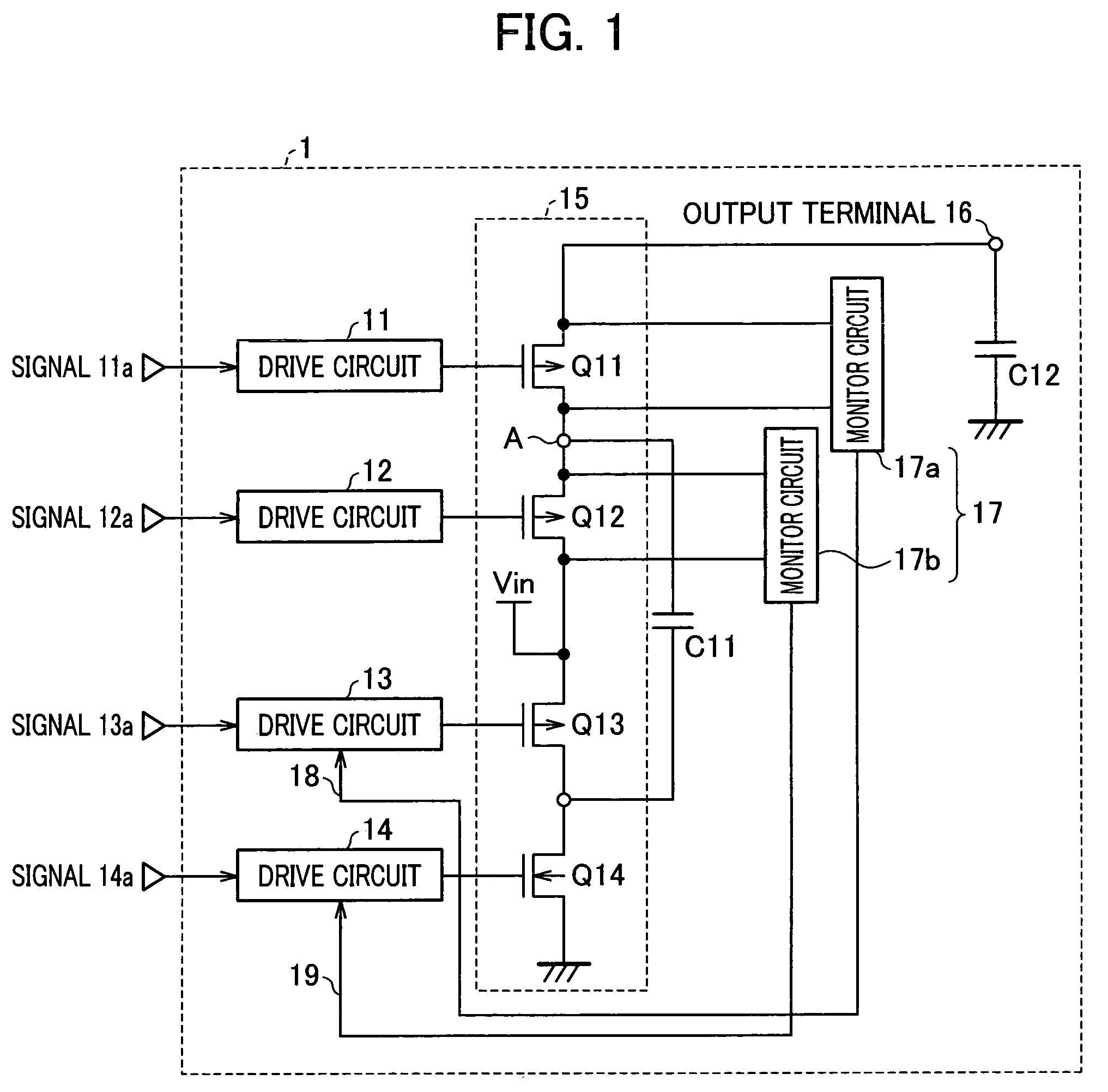
[0061]The present embodiment illustrates a DC / DC converter that performs the step-up using a charge pump. This DC / DC converter is used for stepping up a power supply voltage Vin in, for example, a small electronic device. This converter controls a pulsed voltage applied to a capacitor. On this account, a large current instantly flows at the time of, for example, the pulse rise or fall, in a case where the voltage of the output capacitor decreases either in the initial state (e.g. power-on) or on account of load fluctuation. This may cause crashing of the system. It is noted that conventional arts provide an initial standby state for a period immediately after the power-on. The charge pump starts after this initial standby state. The present embodiment prevents an extremely large current termed rush current or peak current from flowing at the time of the charge pump.

[0062]As shown in FIG. 1, a charge pump circuit 1 (charge pump DC / DC converter) includes a charge pump SW circuit 15, d...

embodiment 2

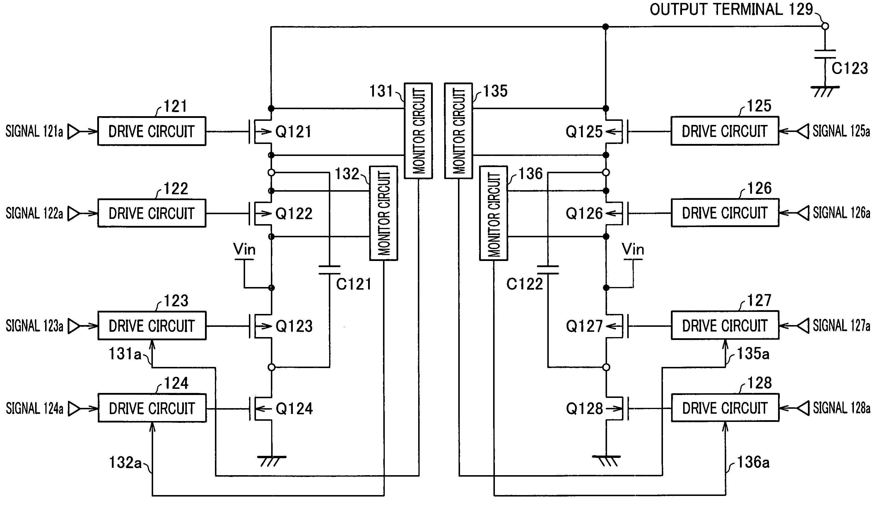
[0142]Embodiment 1 described how the rush current and peak current at the time of the charge pump of a charge pump circuit are restrained. Incidentally, since a charge pump circuit is a power supply circuit, it is necessary to consider a ripple of the output voltage, in addition to the aforesaid rush current and peak current.

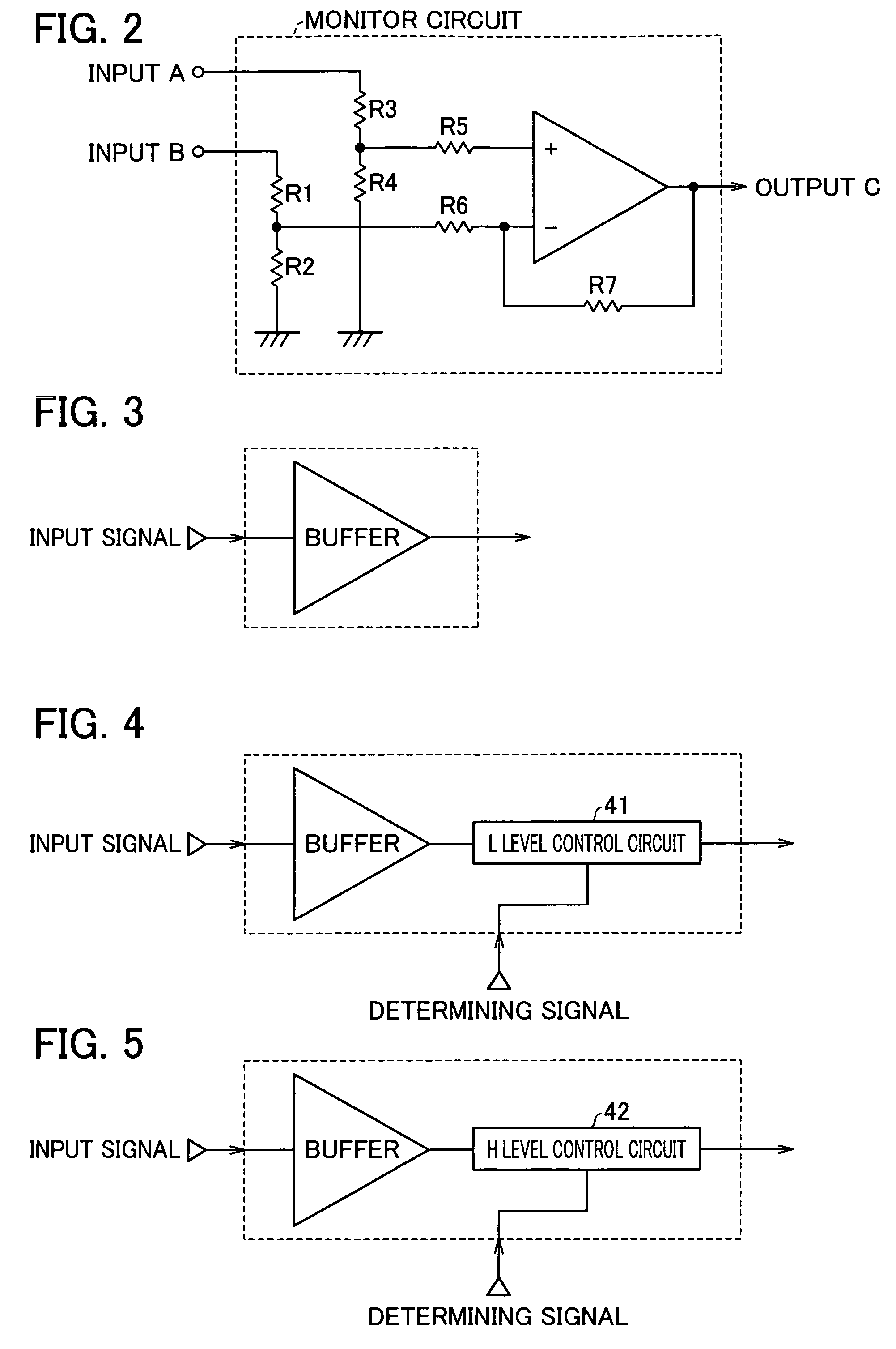
[0143]A charge pump circuit 210 of Embodiment 2 includes the charge pump circuit 1 of Embodiment 1 and an output voltage monitor circuit 205 for reducing an output ripple. The output voltage monitor circuit 205 restrains the output voltage of the charge pump circuit 210 to be not higher than a predetermined level, in a case where the switches Q11 and Q13 are turned on while the switches Q12 and Q14 are turned off (i.e. in a second period; discharge period, predetermined period). This makes it possible to eliminate a drop voltage in the discharge period. That is, it is possible to minimize a drop voltage (ripple voltage) that occurs in the drive period (charge pe...


PUM


Abstract

A charge pump DC / DC converter circuit of the present invention includes: a monitor circuit that detects a potential difference between terminals of a semiconductor switch that turns on during a first period, so as to output a determining signal corresponding to the potential difference; and each of drive circuits that outputs a drive signal to a semiconductor switch that turns on during a first period, in response to the determining signal. The drive signal increases the on-resistance of the semiconductor switch in proportion to the detected potential difference.

Description

[0001]This Nonprovisional application claims priority under 35 U.S.C. § 119(a) on Patent Application No. 049656 / 2005 filed in Japan on Feb. 24, 2005 and Patent Application No. 043057 / 2006 filed in Japan on Feb. 20, 2006, the entire contents of which are hereby incorporated by reference.FIELD OF THE INVENTION[0002]The present invention relates to a DC / DC converter circuit that converts a direct current to a predetermined direct current, and particularly relates to a charge pump DC / DC converter circuit.BACKGROUND OF THE INVENTION[0003]An example of a conventional charge pump DC / DC converter circuit is shown in FIG. 34. This circuit is a double step-up charge pump circuit that outputs a voltage twice as much as a power source voltage Vin. As shown in the figure, the DC / DC converter includes a charge pump SW circuit 55, drive circuits 51–54, step-up capacitor C51, and an output capacitor C52. The charge pump SW circuit 55 is made of semiconductor switches Q51–Q54 each being a MOS transi...

Claims


Application Information

Patent Timeline
Patent Type & Authority Patents(United States)
IPC IPC(8): H02M3/07H02M3/18
CPCH02M3/07
Inventor KAISHITA, KENJIDOI, HIROKI
Owner SHARP KK
Why Eureka
Try Eureka