
Method and apparatus for accessing a dynamic memory device by providing at least one of burst and latency information over at least one of redundant row and column address lines

a dynamic memory device and burst and latency technology, applied in the field of dynamic memory devices, can solve the problems of inability to change the operation mode of the memory device without, the operation mode of the memory device cannot be substantially altered concurrently with an access command, and the time-consuming process of changing the operation mode of the memory devi

Active Publication Date: 2007-05-29
MICRON TECH INC
View PDF10 Cites 47 Cited by
  • Summary
  • Abstract
  • Description
  • Claims
  • Application Information

AI Technical Summary

Benefits of technology

The present invention provides a method, apparatus, and system for accessing a dynamic memory device by receiving a command from a controller, providing burst length information and latency information in response to the command, and accessing the memory based on the burst length information and latency information. This allows for faster and more efficient access to the memory, improving the overall performance of the system.

Problems solved by technology

While a semiconductor memory device may be capable of supporting multiple modes of operation (i.e., different latency levels and / or burst lengths), as a general matter, the operation mode of the memory device cannot be altered without reprogramming its mode register.
Changing the operation mode of the memory device, however, may be a time consuming process, as the reprogramming must be loaded (or reloaded) when all memory banks are idle and no bursts are in progress.
Additionally, in conventional memory devices, the operation mode of the memory device cannot be altered substantially concurrently with an access command (e.g., read command and write command).
This may result in power wastage, as multiple commands may be needed to change the operation mode of the memory device and to access the contents of the memory device.

Method used


Image

  • Method and apparatus for accessing a dynamic memory device by providing at least one of burst and latency information over at least one of redundant row and column address lines
  • Method and apparatus for accessing a dynamic memory device by providing at least one of burst and latency information over at least one of redundant row and column address lines
  • Method and apparatus for accessing a dynamic memory device by providing at least one of burst and latency information over at least one of redundant row and column address lines

Examples


Embodiment Construction

[0023]Illustrative embodiments of the invention are described below. In the interest of clarity, not all features of an actual implementation are described in this specification. It will of course be appreciated that in the development of any such actual embodiment, numerous implementation-specific decisions must be made to achieve the developers' specific goals, such as compliance with system-related and business-related constraints, which will vary from one implementation to another. Moreover, it will be appreciated that such a development effort might be complex and time-consuming, but would nevertheless be a routine undertaking for those of ordinary skill in the art having the benefit of this disclosure.

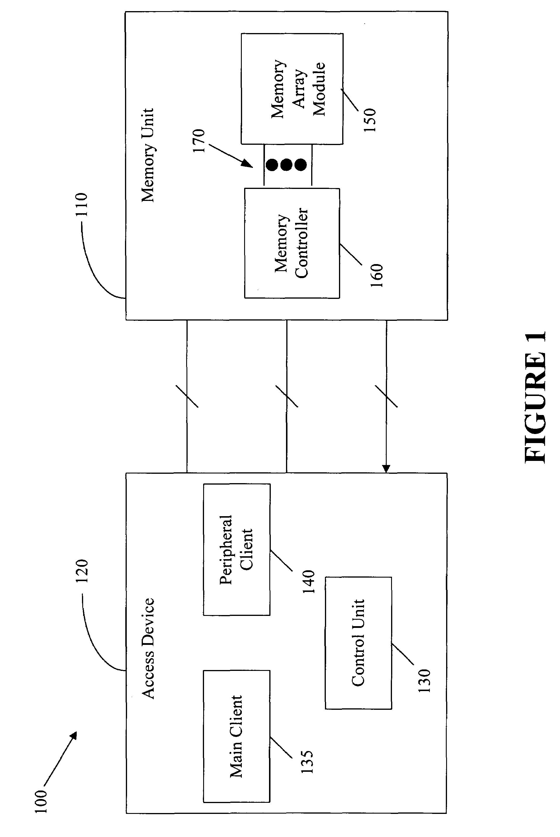
[0024]Referring to FIG. 1, a block diagram of a system 100 is illustrated, in accordance with one embodiment of the present invention. The system 100 comprises a memory unit 110 capable of storing and retrieving data, which may be accessed by a device 120. The access device 120 c...


PUM


Abstract

A method and apparatus are provided for accessing a dynamic memory device. The method comprises receiving a command from a controller to access a memory, receiving, from the controller, at least one of burst length information and latency information in association with the command to access the memory; and providing data to or from the memory in response to the command based on at least one of the burst length information and the latency information.

Description

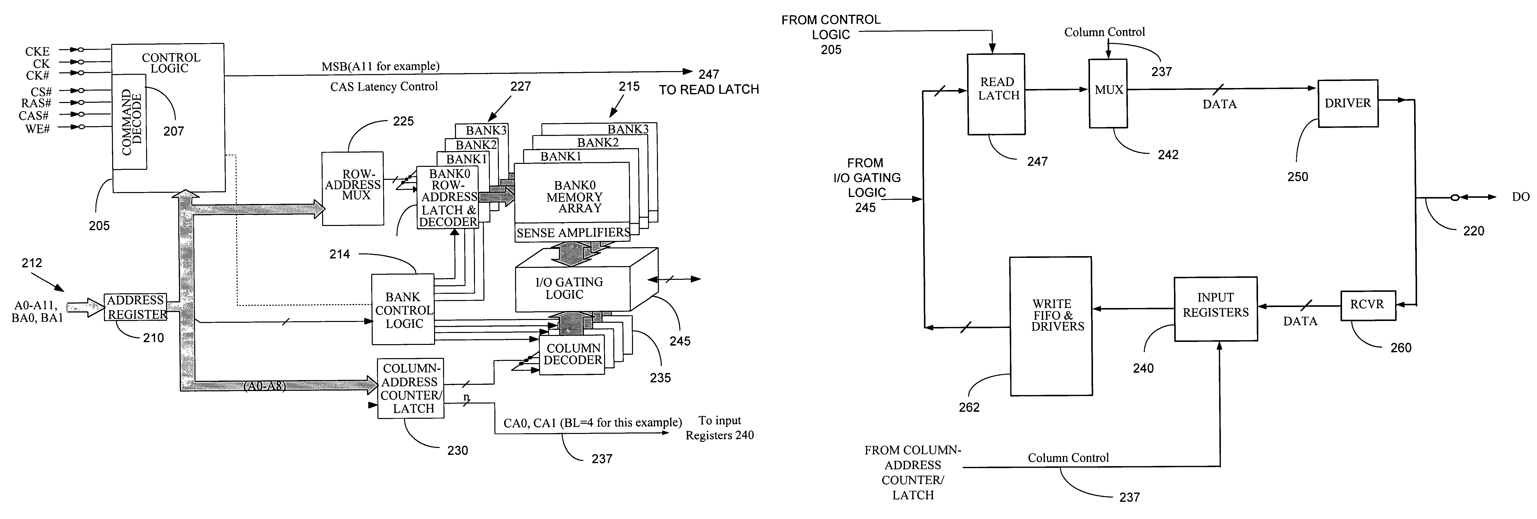
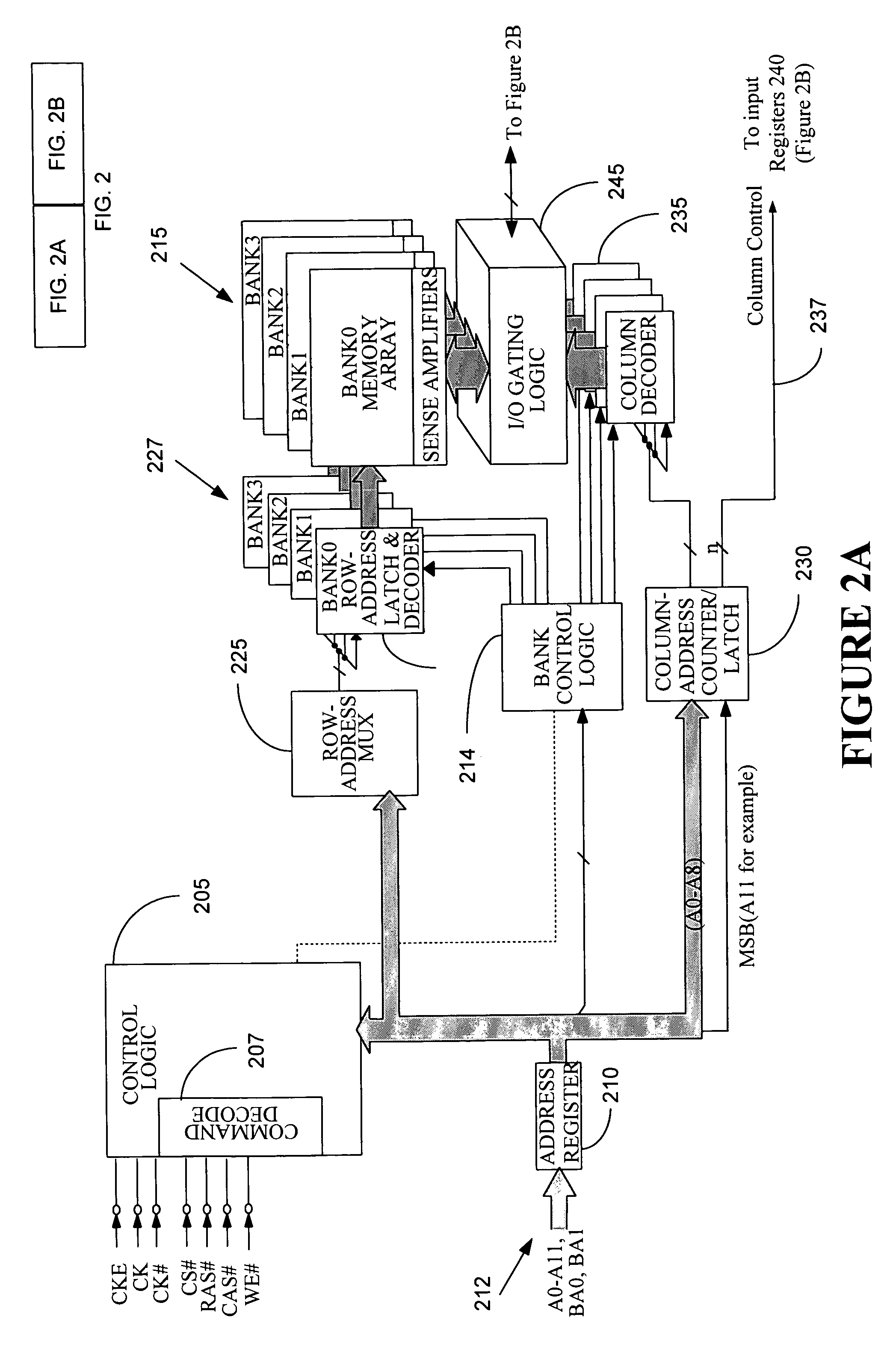
BACKGROUND OF THE INVENTION[0001]1. Field of the Invention[0002]This invention relates generally to dynamic memory devices, and, more specifically, to a dynamic memory device adapted to be accessed with an adjustable burst length, column address strobe (CAS) latency, and / or write latency.[0003]2. Description of the Related Art[0004]Generally, there are at least two types of data transfers to and from memory. A first type includes a data transfer for a main client that requires large amounts of data to be transferred to and from the memory. A second type of data transfer is for a peripheral client that typically requires small amounts of data to be transferred to and from the memory.[0005]To allow greater flexibility for data transfers, many of today's dynamic memory devices, such as Synchronous RAM (SDRAM), double data rate SDRAM devices (DDR SDRAM), Rambus™ DRAM (RDRAM) and the like, are usually designed to operate at various latency levels and burst lengths. For example, a semicon...

Claims


Application Information

Patent Timeline
Patent Type & Authority Patents(United States)
IPC IPC(8): G06F13/00G06F13/28G11C7/10
CPCG11C7/1018G11C7/1072
Inventor CHOI, JOO S.
Owner MICRON TECH INC
Learn More